Designing and manufacturing electronic boards

Designing and manufacturing electronic boards

If you prototype printed circuit boards , how can you ensure that laminates and prepregs you used will match those used in offshore volume production?

As an industry, those of us involved in designing and manufacturing electronic products can all agree that we now live and operate in a global supply chain environment. Since a lot of what is incorporated into current and next generation products is reflected in the software, this isn’t much of a concern. Take your favorite products, download the latest software update and newly developed apps and you’re ready to go.

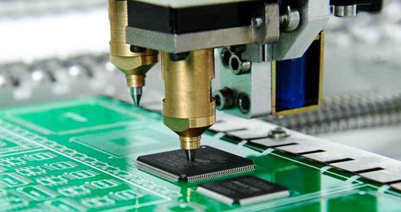
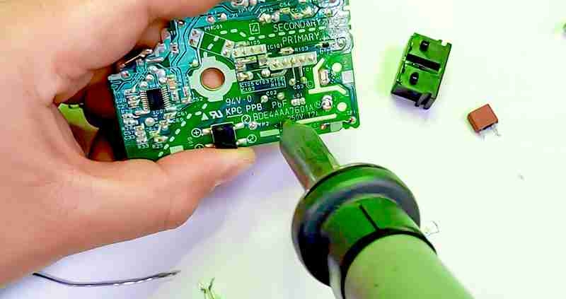
When it comes to developing the pieces of hardware, the process is not so simple. And, when it comes to printed circuit board (PCB) development efforts, the process becomes even more challenging. That’s because PCBs are the launching points for hardware product development and the laminate and prepreg materials used in designing and manufacturing PCBs are the nuclei for those boards. (Prepreg is fiberglass cloth that has been saturated with resin that is not fully cured. As a PCB is placed under the heat and pressure of lamination this resin melts and flows into the voids in the adjacent copper layers filling them.)

  • Gerber data, which board and stencil manufacturers still depend on for their processes. There will be a point when this is not required. Depending on your vendor base, that time may or may not be now.
  • Valor ODB++, which  allows board and stencil manufacturers to gain insight into the design and offer feedback to improve processes, thus reducing production cost over time. It also allows use of Valor DFA software for reviewing an assembly to improve yields in production by PCB manufacturers with that level of sophistication. Since it can be used for programming pick-and-place lines, it could be a “one file” approach to all manufacturing requirements.
  • CAD ACSII database, which supports the fastest approach to programming the pick-and-place lines and can support other programming efforts such as AOI.
Why SMT

Why SMT?

Surface-mount technology (SMT) is a method for producing electronic circuits in which the components are mounted or placed directly onto the surface of printed circuit boards (PCBs). An electronic device so made is called a surface-mount device (SMD).

An SMT component is usually smaller than its through-hole counterpart because it has either smaller leads or no leads at all. It may have short pins or leads of various styles, flat contacts, a matrix of solder balls (BGAs), or terminations on the body of the component.

Why SMT?

Mass produced electronic circuit boards need to be manufactured in a highly mechanised manner to ensure the lowest cost of manufacture. It need passive SMDs (Resistors and capacitors),Transistors and diodes, Integrated circuits should be packaged in reels / Reels.

PCB Production Steps

PCB production Steps

PCB Etching Process

All PCB’s are made by bonding a layer of copper over the entire substrate, sometimes on both sides. Etching process has to be done to remove unnecessary copper after applying a temporary mask, leaving only the desired copper traces.

Though there are many methods available for etching, the most common method used by electronics hobbyists is etching using ferric chloride ir hydrochloric acid. Both are abundant and cheap. Dip the PCB inside the solution and keep it moving inside. Take it out at times and stop the process as soon as the copper layer has gone. After etching, rub the PCB with a little acetone to remove the black colour, thus giving the PCB a shining attractive look. The PCB layout is now complete.

PCB Drilling

The components that have to be attached to the multi-layered PCB can be done only by VIAS drilling. That is, a pated-through hole is drilled in the shape of annular rings. Small drill bits that are made out of tungsten carbide is used for the drilling. A dremel drill press is normally used to punch the holes. Usually, a 0.035 inch drill bit is used. For high volume production automated drilling machines are used.

Sometimes, very small holes may have to be drilled, and mechanical methods may permanently damage the PCB. In such cases, laser drilled VIAS may be used to produce an interior surface finish inside the holes.

Conductor Plating

The outer layer of the PCB contains copper connections (the part where the components are placed) which do not allow solderability of the components. To make it solderable, the surface of the material has to be plated with gold, tin, or nickel.

Solder Resist

The other areas which are not to be solderable are covered with a solder resist material. It is basically a polymer coating that prevents the solder from bringing traces and possibly creating shortcuts to nearby component leads.

PCB Testing

In industrial applications, PCB’s are tested by different methods such as Bed of Nails Test, Rigid Needle adaptor, CT scanning test, and so on. The basic of all tests include a computer program which will instruct the electrical test unit to apply a small voltage to each contact point, and verify that a certain voltage appears at the appropriate contact points.

Basic process to assembly PCB board with components

Basic process to assembly PCB board with components.

As a China original PCBA manufacturer ,we do PCBA board according to Bom list & Gerber files via SMT machines & DIP assembly.
Below is the basic process to assembly PCB board with components.
1.Confirm the necessary files and order details.
2.Order and receive the SMT paste stencil if necessary.
3.Program our machines from the BOM and Centroid file, before the materials arrive.
4.Materials are received in. Materials are audited before your job is run.
5.If all materials are in before noon, the assembly clock starts that day. If after noon, the clock starts the next day.
6.A SMT stencil and stencil printer are used to mechanically apply the paste.
7.An automatic pick and place machine place the SMT components.
8.A SMT reflow oven is used to reflow the solder onto the SMT components.
9.BGA components are X-rayed to verify placement accuracy and to detect any solder bridges.
10.Thru-hole parts are inserted by hand. They may also be wave soldered depending on the board layout.
11.A 100% final quality check is performed.
12.The finished PC board assemblies are shipped back to you.
C-Alley PCB Assembly & Prototyping services

C-Alley PCB Assembly & Prototyping services

C-Alley’s offers PCB prototyping services utilizing dedicated automated pick and place equipment for samples making & mass production for high quanlity PCBA circuit board.
A distinguishing feature of C-Alley’s turnkey manufacturing solutions is our Transparent Pricing. Open BOM to list the cost of each components, you can check our profit point only wthin 5~10%, Transparent Pricing includes a line by line costing of the Bill of Materials, labor costs, profit margins. It’s truly open-book pricing. It allows AMI and its customers to work jointly at reducing costs which make everyone more successful in the end.

As a  PCBA manufacturer ,we ensure 99.7% workable PCBA, but 100% yeild by function testing, but how can we guarantee such high passing rate ? modern high-tech PCBAs can potentially have 20,000–30,000 solder joints, requiring sophisticated automated inspection techniques to efficiently inspect results and provide process control feedback. The solutions is to set up a series testing instructions such as programming and function test.

 In a high-mix environment C-Alley typically deploy automated optical inspection (AOI), automated x-ray inspection(AXI), and flying probe (FP). By endeavoring to minimize test element overlap, we minimize both programming and runtimes.
Our strengths
Surface Mount, Through-Hole, or Mixed Technologies
BGA placement down to 0.2mm pitch
Chip placement down to 0201,01005 packages
Machine-placed prototypes,PCB prototypes
IPC-610 Class III Workmanship with certified in-house trainer
Extensive automated production equipment
X-Ray and Automated Optical Inspection for BGA
Coating and Encapsulation Services
Why the etch pads are not big enough for vias

Why the etch pads are not big enough for vias

Now C-Alley is using the leading edge technologies such as ball-grid arrays (BGAs), chip scale packaging, flip chips, QFNs, DFNs, and others. It shines x-ray radiation through a component package like a BGA to view images including wire bonding, solder joints, and solder defects, if any. Standard x-ray inspection is used for simple applications, whereas high-end x-ray is used to detect such defects as head-on-pillow, disjointed balls on a BGA package, wire bonding damage, and other similar problems.

C-Alley is a PCBA manufacturer who is dedicated to offering high quality PCBA products to worldwide customers. Please send us your Gerbers and BOM,we’ll quote for your A.S.A.P.

Today we’re going to discuss about the problem that why the etch pads are not big enough for vias?

As designs get more compressed, conductors, spaces and pads continue their march to be smaller and smaller. Designers are left trying to squeeze pad sizes in order to route traces within BGAs or other tight component packages.

There is often confusion related to drawing requirements for drilled holes and the sizes manufacturers actually drill to achieve the drawing requirements. Let’s clear that up and talk about strategies to gain as much room as possible, while maintaining adequate annular ring.

First, let’s not forget fillets at the via-to-trace transition. This is absolutely required, especially if Class 2 annular ring is called out. It provides a level of insurance against breakout at the via-to-pad transition, which could lead to an open circuit. It is also good design practice, as it improves etch quality and provides mechanical strain relief, reducing potential for cracking.

So what’s the deal with drilled holes? We will concentrate here on mechanically drilled holes, not laser microvias. (That is a topic for another day.) When a drawing calls out a hole size, it will usually have a tolerance, such as 0.010″+/-0.003″. When this happens, the PCB manufacturer must select a drill size that compensates for all processing so the finished hole will meet the drawing requirement. The manufacturer will aim for the center of the drawing window, so in the case of 0.010″+/-0.003″ they will try to finish at 0.010″ or slightly above that. If the tolerance is not centered on the nominal hole – e.g., 0.010″+0.002″/-0.004″ – they will aim for the middle of the range, in this case 0.009″.

To make this work, they will add allowances for copper plating and final finish to the finished size. Typically, they will drill about 0.002″ to 0.003″ above the maximum allowable finished hole size. In the case of our example, they will drill at 0.015″.

This eats into the annular ring, especially for the internal layers. Say you designed a 10 mil pad and coupled that with a 20 mil pad, and thought you had plenty of room. However, the internal layers are now down to 2.5 mils of annular ring at design. Making IPC minimums for internal annular ring on the finished product will be unlikely.

De-soldering PCB components

De-soldering components (through-hole and SMD)

SMT parts have many advantages over their older through hole ancestors, namely: smaller size, lower cost manufacturing costs, and less likelihood of obsolescence. However, an often overlooked advantage is the ease at which surface mount components can be soldered and desoldered. At first this might seem like a controversial subject, but it isn’t to engineers and technicians to have grown accustomed to working with both types of parts. Just try desoldering a 16 pin DIP from a PCB with a solder sucker without ripping a trace, and you’ll understand how hard reworking a through hole part can be. Compare this to a desoldering a 16 pin SOIC which can be removed in a matter of seconds with no special equipment.

Vacuum Desoldering

The vacuum based through-hole desoldering station consisted of a soldering iron with a hollow tip and body which leads to a glass tube capped by a filer at one end which is also the end the vacuum is applied to. The trick is to heat up the whole solder joint (I use an ample amount of flux to assist) and then start the vacuum by pulling the trigger. During this time I am also wiggling the soldering iron tip in order to break the component pin free from the wall of the hole or plate-through. Done correctly both the PCB and the component being removed are reusable.

Infrared Desoldering

The infrared based system, referred to as an Infrared Welder by the manufacturer, can ultimately heat a smaller area to a hotter temperature than hot air, or so I believe. To mask off the surrounding area for hot air you need to keep your airflow low and redirect it away from the rest of the PCB. To redirect Infrared you use the reflective properties of aluminum foil. It’s then mostly a matter of firing up the fume fan and having the patience to wait for the direct heat to do the job. Again a judicious use of flux helps.

Hot Air Desoldering

Hot Air is similar in that flux helps, fumes and smoke may be present and you have to have the patience to wait for the part to come fully loose — half loose doesn’t cut it. To this end I recommend a hot air holder, a fume fan and an egg timer. If you don’t have an egg timer I am sure there is an app for that somewhere.

Desoldering with Chip Quik and an iron

I have found The quickest way to desolder SMT without investing in any of this equipment is to use a product which lowers the melting point of the solder metal when mixed with it as it allows a soldering iron to melt the entire chip’s footprint simultaneously allowing it to be removed.

CAM350 files

CAM files

PCB Manufacturing

For over 10 years C-Alley has been a leading provider of gerber viewing, editing and CAM software. Now C-Alley’s main service turn PCB assembly into PCB Design with special functions.

We use CAM350 to edit & view Gerber files, and make production files.

The data files used directly in the manufacture of printed wiring. The file types are: (1) Gerber files, which control a photo-plotter. (2) NC Drill file, which controls an NC Drill machine. (3) Fabrication drawings in Gerber, HPGL or any other electronic format. Hard copy prints may be available also. CAM files represent the final product of PCB design. These files are given to the board house which further refines and manipulates CAM in their processes, for example in step- and-repeat panelization

2016 China Printed Circuit Board (PCB) Industry

2016 China Printed Circuit Board (PCB) Industry

The China Printed Circuit Board (PCB) Industry 2016 Market Research Report is a professional and in-depth study on the current state of the Printed Circuit Board (PCB) industry.

The China Printed Circuit Board Industry provides a basic overview of the industry including definitions, classifications, applications and industry chain structure. The Printed Circuit Board market analysis is provided for the international markets including development trends, competitive landscape analysis, and key regions development status. Development policies and plans are discussed as well as manufacturing processes and cost structures are also analyzed. This report also states import/export consumption, supply and demand Figures, cost, price, revenue and gross margins.

Over the five years through 2016, revenue for the Printed Circuit Board Manufacturing industry has increased at an average annualized rate of 8.1% to $78.9 billion. As printed circuit boards are intermediate components, the majority of industry revenue is derived from sales to downstream wireless industries and consumer electronic manufacturing industries. Growing household income in China has led to increasing demand for electronic products, boosting demand for printed circuit boards.

Growth in the Printed Circuit Board Manufacturing industry in China has gradually slowed in recent years. In 2016 alone, industry revenue is expected to grow 6.5%.

The Printed Circuit Board Manufacturing industry has grown rapidly over the past five years. In 2016, industry revenue is expected to reach $78.9 billion. High growth has been driven by greater domestic and foreign demand.

As printed circuit boards are an intermediate product, the majority of industry revenue is derived from sales to downstream wireless industries and consumer electronic manufacturing industries. Growing household income in China has led to increasing demand for electronic products, creating demand for printed circuit boards. However, wireless and consumer electronics industries are subject to rapid technological change, which brings about intense competition, short product life cycles and significant fluctuations in product.

PCB practical certifications

A PCBA leader with certifications

C-Alley is a Chinese PCBA leader and one of the leading assember of high-value/requrements printed circuit boards . The core business segments are Smart home application Devices, Automotive, Industrial, Medical and Advanced Packaging. In 2016, C-Alley has extened the global presence to Austria, Europe, USA, The Middle East and Russia.  our factory bring an enviable number of quality approvals and certifications including ISO 9001, ISO 1400 and ISO/TS 16949, full UL Recognition.

Now we’ll focus on the production tech of extremely compact substrates/modules, advanced heat management, Embedded Component Packaging , HF printed circuit boards (PCBs) and flexible PCBs for medical devices .

Welcome to send a quote to :  [email protected] , and better to attach Gerber file & Bom list, thank you!

Sitemap | ©Copyright 2023 H.K C-Alley Co., LTD. | Alibaba | KingshengPCBA | All Rights Reserved