HDI PCB
HDI (High-Density Interconnect PCB) is commonly used in applications such as smartphones, tablets, wearable devices, medical equipment, aerospace systems, and automotive electronics. C-Alley has specialized in providing customers with advanced HDI PCB design and manufacturing techniques and high-quality products.
HDI PCB (High-Density Interconnect PCB) contains blind and/or buried vias and often contains micro vias of .006 or less in diameter. They have a higher circuitry density than traditional circuit boards.
HDI PCBs are characterized by high-density attributes including laser microvias, fine lines, and high-performance thin materials. This increased density enables more functions per unit area. Higher technology HDI PCBs have multiple layers of copper-filled stacked microvias (Advanced HDI PCBs) which creates a structure that enables even more complex interconnections. These very complex structures provide the necessary routing solutions for today’s large pin-count chips utilized in mobile devices and other high-technology products.
HDI Structures: 1+N+1 – PCBs contain 1 “build-up” of high-density interconnection layers; i+N+i (i≥2) – PCBs contain 2 or more “build-up” of high-density interconnection layers.
Key features of HDI PCB include:
High density: HDI PCBs use smaller vias and micro vias, allowing for increased circuit density and reduced size. This enables the placement of more components in a smaller area.
Miniaturization: HDI PCBs allow for the use of smaller and more tightly packed components, resulting in smaller and lighter electronic devices.
High-speed performance: The shorter trace lengths and reduced signal interference in HDI PCBs enable better signal integrity, making them suitable for high-speed and high-frequency applications.
Multiple layers: HDI PCBs often have multiple layers, including stacked vias and buried vias, which provide additional routing options and increased design flexibility.
Improved thermal management: HDI PCBs can incorporate thermal vias and copper-filled micro vias to enhance heat dissipation and thermal management in compact designs.
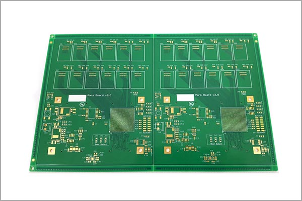
Layers:4L
Thickness: 1.6mm
Min Hole Size: 0.1mm
Min Line Width: 0.076mm
Copper Thickness: 1oz
Surface Finishing: ENIG
Molding Tolerance:+/-0.05mm
HDI Structures: 1+N+1
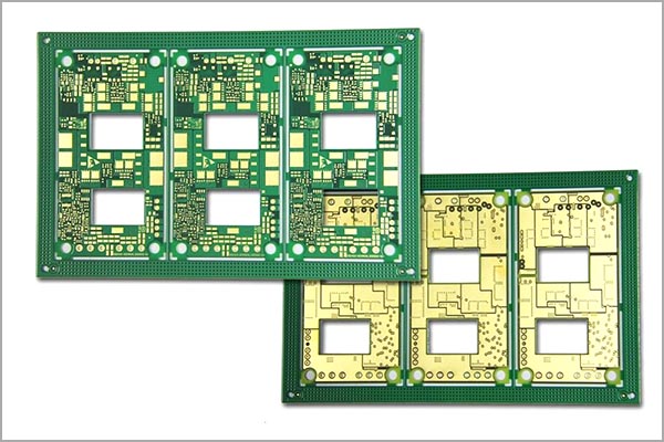
Layers: 6L
Thickness: 1.2mm
Min Hole Size: 0.1mm
Min Line Width: 0.1mm
Copper Thickness: 1oz
Surface Finishing: ENIG
Molding Tolerance:+/-0.05mm
HDI Structures: 2+N+2
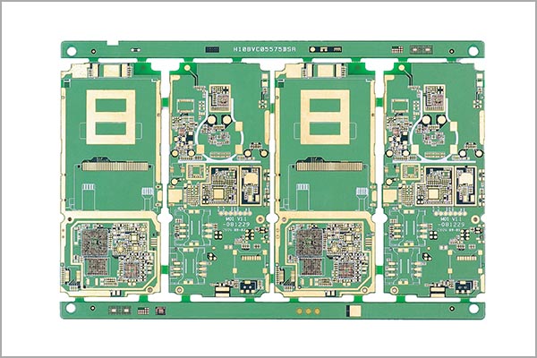
Layers: 8L
Thickness: 0.1mm
Max Length: 1265mm
Min Line Width: 0.1mm
Copper Thickness: 1oz
Surface Finishing: ENIG
Molding Tolerance:+/-0.05mm
HDI Structures: 3+N+3
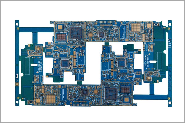
Layers: 8L
Thickness: 1.6mm
Min Hole Size: 0.15mm
Min Line Width: 0.1mm
Copper Thickness: 1oz
Surface Finishing: ENIG
Molding Tolerance: +/-0.05mm
HDI Structures: 4+N+4
HDI Production Capability
| Item | Standard | Advanced |
| Max.Layer count | 30 | 32 |
| Products type | ELIC(4+2+4)、HDI | ELIC(4+2+4)、HDI |
| Min. Drill Size | 0.15mm | 0.15mm |
| Min. Laser Drill Size | 0.10mm | 0.075mm |
| Min.BGA Pitch | 0.40mm | 0.20mm |
| Impedance Control Tolerance | ± 8% | ± 5% |
| Buried Vias and Blind Vias | Yes | Yes |
| Stacked Via | Yes | Yes |
| Copper Filled Microvia | Yes | Yes |
| HDI Structure 1+N+1 \ 2+N+2\3+N+3 |
Yes | Yes |


