C-Alley Technology News is the sharing of knowledge, experience, and tips about PCB assembly technology on a blog. This sharing can cover a variety of technical fields, including PCB design, PCB fabrication, PCB assembly, electronic assembly, EMS, and more.

PCBA SMT processing lead time

PCBA SMT processing lead time

Understanding the cycle of PCBA SMT processing is crucial, as both companies and individuals need to make reasonable arrangements in terms of time.

PCBA SMT processing lead time

PCBA processing is a complex process involving multiple processes and links, and its lead time is influenced by multiple factors.

Firstly, the production lead time of PCBA SMT processing depends on the complexity and scale of the project. Generally speaking, more complex projects require longer time to complete.

Secondly, the reliability and stability of the supply chain also have a significant impact on the PCBA SMT processing lead time. If there is a delay or malfunction in the supply chain, it will directly lead to an extension of the processing lead time.

Therefore, it is recommended to pay attention to the supply chain management capabilities of PCBA processing manufacturers and choose reputable manufacturers for cooperation.

In addition, the PCBA SMT processing lead time is also constrained by customer demand and delivery time. Some customers may have urgent delivery requirements and need to complete the processing in a short period of time. In this situation, manufacturers need to adjust their production plans and resources as much as possible to meet customer needs. Therefore, it is very important to communicate delivery time requirements in a timely manner when negotiating cooperation with PCBA manufacturers.

In addition, some technical challenges may also lead to an extension of the PCBA SMT processing lead time. Therefore, in the PCBA SMT processing project, timely resolution of technical issues is the key to ensuring the processing cycle.

In summary, the lead time of PCBA SMT processing is influenced by multiple factors. In order to reduce processing lead time, it is recommended to choose a reliable supply chain, actively communicate delivery time requirements with manufacturers, and promptly solve technical problems. Only by comprehensively considering these factors can we ensure that the PCBA processing lead time is as short as possible.

Since 2008, H.K C-alley Tech Co., Ltd provides a One-stop PCB Assembly Service and Electronics Manufacturing Service (EMS) in Bao’an District Shenzhen, China. As an ISO 9001, UL, CSA, and CCC certified manufacturer, We offer flexible, cost-effective, and high-quality EMS solutions for printed circuit board assembly (PCBA) and complete product assembly through state-of-the-art manufacturing technologies and production facilities. With over 15 years of manufacturing experience in the electronics sectors, C-alley become a highly reliable PCB assembler for ODM Design and Electronics Reverse Engineering.

PCB Assembly approaches

Three Approaches to Ensure PCBA Assembly Service Completed

Circuit boards are present in almost all electronic devices you use, and while they are common, it doesn’t mean they are simple. SMT production of circuit boards is a complex business, and to assemble them correctly, you need the right tools, the right parts, and the right expertise. Entrusting professionals to do the assembly means ensuring quality control measures are followed throughout the process and testing is done, so you can rest assured that when you receive the PCB, it will function as needed. But what is the process for PCB assembly? Do you simply need to let the company know what you need, or do you need to submit every single component? C-Alley takes you through one of three different PCB assembly approaches to order your components.

PCB Assembly approaches

Turnkey PCB Assembly

Choosing turnkey printed circuit board assembly in an SMT factory is a great solution for any business. With this option, our professionals will gather all the necessary parts and assemble the PCB. This PCB assembly solution is cost-effective and helps save time, as we will ensure we have everything needed for the correct build.

Partial/Outsourced PCB Assembly

Partial & Consign PCB Assembly

For those who know exactly what PCB they want but may not have the time or equipment to do the assembly themselves, partial printed circuit board assembly is a perfect choice. You can purchase all the components and parts you want and need, and our experts will use each one during the PCB assembly. This can help you better control production costs and understand the expected outcome of the finished printed circuit board.

Combo PCB Assembly

In SMT assembly, you may know that you need to use certain components in the PCB but still need some parts to complete your PCB electromechanical assembly – this is where combo PCB assembly comes in. You provide us with the parts and components you have, and we will provide anything else you may still need and professionally assemble them together. This option still allows you to have some control over production costs and combines the ease and time-saving features of the C-Alley team to control the most critical components to get the job done.

Precautions in the Process of Prototype PCB Manufacturing

PCB (Printed circuit boards) are an important part of almost all electronic devices used in our daily lives. As such an important component, most OEMs require sophisticated PCB design and manufacturing, which is because they cannot withstand any failure when used in applications. However, we can always avoid some invisible problems and small errors, which pose a certain threat to the function of the PCB board. This is when the prototype PCB manufacturing becomes particularly important, it is an early sample of the circuit board, and its sole purpose is to check the full functionality of the PCB design. Although it may seem like an extra step, a prototype PCB performs a pre-production analysis of the board before you begin a full production run. Let’s analyze why PCB prototypes are so important in the manufacturing process.

pcb prototype

  • Accelerate the overall prototype PCB manufacturing:
    Highly accurate PCB prototypes help minimize iterations and rework that can occur during the production phase. Prototyping allows defects to be detected at an early stage, giving manufacturers enough time to correct them before actual production. In addition, with PCB prototypes, it is easier for manufacturers to communicate with customers and let them understand the key design elements. In fact, customers can also request changes or modifications, which can be time-consuming in the later stages of production.
  • Test:
    The PCB prototyping process is not just a random error detection process. On the other hand, it is a key step, including several test processes, such as temperature change test, power change test, shock resistance test, etc. All of these tests check the board’s ability to operate in harsh environmental conditions. Designers also scrutinize all components and their functions to make sure they work as expected. This tiny inspection allows the PCB to be created faster and more accurately during actual production runs.
  • Minimize costs:
    Early detection of errors helps vendors correct errors easily and promptly at the lowest cost. This is not the case when a fault is discovered during the production phase. Finding design flaws at a later stage requires huge sums of money to fix them. This will in turn fully impact the project budget and schedule. In addition, PCB prototyping allows manufacturers to arrange materials and components in advance according to design specifications. They can also find and test cost-effective components, materials, and assembly methods. Overall, prototyping minimizes the last-minute rush to purchase materials while enabling them to make appropriate decisions about manufacturing methods.

Prototype PCB helps board manufacturers and customers have a clear idea of lead times, prices, and potential component inventory issues. This leads to improved and more efficient PCB processing. Prototype PCB allows board factories to experiment with different designs and components and select the best and most suitable at a budget-friendly price. This process helps give partners a clear understanding of what to expect from production operations. It allows projects to be completed efficiently with minimal material loss, expense, and effort. Needless to say, circuit board proofing is a good way to measure the functionality of the final product.

SMD Package

SMD Packaging Technology: Exploring Different Types and Their Significance

Introduction to SMD Packaging

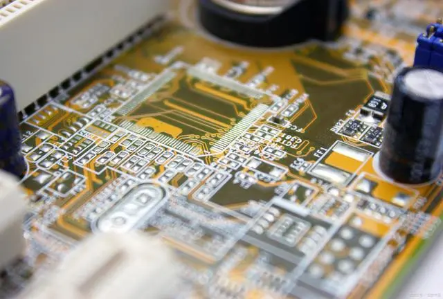
SMD packaging technology is an abbreviation of Surface Mounted Devices packaging technology, meaning: Surface Mount devices, it is one of the Surface Mount Technology (SMT) components. In the initial stage of the production of electronic circuit boards, through-the-hole assembly is completely completed manually. When the first automated machines were introduced, they could place some simple pin components, but complex components still needed to be placed manually for wave soldering. Surface Mounted components (Surface Mounted components) are mainly rectangular chip components, cylindrical chip components, composite chip components, and shaped chip components.

SMD Package

SMD package

In the initial stage of the production of electronic circuit boards, the hole assembly is completely completed manually. When the first automated machines were introduced, they could place some simple pin components, but complex components still needed to be placed manually for wave soldering.

What are the types of SMD packaging technology? _ Common Packaging Types

  1. ball grid array (BGA)

    Spherical contact display, one of the surface mount type packages. A spherical convex point is made on the back of the printed substrate according to the display mode to replace the pin, and the LSI chip is assembled on the front of the printed substrate, and then sealed with molded resin or potting method. Also known as raised point display carrier (PAC). The pin can be more than 200 and is a multi-pin LSI for a package.
    The package body can also be made smaller than the QFP (four-sided pin flat package). For example, a 360-pin BGA with a pin center distance of 1.5mm is only 31mm square; The QFP of pin 304 with a pin center distance of 0.5mm is 40mm square. And BGA doesn’t have to worry about pin distortion like QFP.
    The package was developed by Motorola in the United States and was first adopted in devices such as portable phones and is likely to be popularized in personal computers in the United States in the future. Initially, the BGA had a pin (raised) center distance of 1.5mm and a pin number of 225. There are also some LSI manufacturers now developing 500-pin BGA.
    The problem with BGA is the appearance inspection after reflow soldering. It is not clear whether the appearance inspection method is effective. Some believe that due to the large center distance of the welding, the connection can be regarded as stable and can only be handled by functional inspection.
    The American Motorola company calls the package sealed with molded resin OMPAC, and the package sealed by potting method GPAC (see OMPAC and GPAC).

  2. BQFP (quad flat package with bumper)

    Four-sided pin flat package with cushioning. One of the QFP packages provides bumps (cushioning) at the four corners of the package body to prevent the pin from bending and deforming during transport. American semiconductor manufacturers mainly use this package in circuits such as microprocessors and ASICs. The pin center distance is 0.635mm, and the number of pins ranges from 84 to around 196 (see QFP).

  3. butt joint pin grid array (PGA)

    Another name for surface mount PGA (see Surface Mount PGA).

  4. C- (ceramic)

    A mark indicating a ceramic package. For example, CDIP stands for ceramic DIP. It is a sign that is often used in practice.

  5. Cerdip

    Ceramic dual-in-line package sealed with glass for ECL RAM, DSP (digital signal processor), and other circuits. Cerdip with glass window is used for UV-erasing EPROMs and microcomputer circuits with EPROMs inside. Pin center distance 2.54mm, pin number from 8 to 42. In Japan, this package is denoted as DIP-G (G means glass seal).

  6. Cerquad

    One of the surface mount type packages, that is, bottom-sealed ceramic QFP, is used to encapsulate logical LSI circuits such as DSPS. Cerquad with a window is used to encapsulate EPROM circuits. Heat dissipation is better than plastic QFP, and 1.5 ~ 2W power can be allowed under natural air cooling conditions. However, the packaging cost is 3 to 5 times higher than the plastic QFP. The center distance of the pin is 1.27mm, 0.8mm, 0.65mm, 0.5mm, 0.4mm, and other specifications. Pin count from 32 to 368.

  7. ceramic leaded chip carrier (CLCC)

    Ceramic chip carrier with pins, one of the surface mount type packages, pins from the four sides of the package, in a T-shape. A window for encapsulating a UV-erasing EPROM and a microcomputer circuit with an EPROM, etc. This package is also called QFJ, QFJ-G (see QFJ).
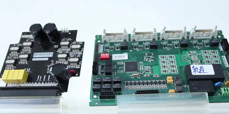
  8. COB (chip on board)

    On-board chip packaging is one of the bare chip mounting technologies. The semiconductor chip is attached to the printed circuit board, the electrical connection between the chip and the substrate is realized by lead stitching, and the electrical connection between the chip and the substrate is realized by lead stitching, and the resin is covered to ensure reliability. Although COB is the simplest bare-chip mount technology, its package density is far less than TAB and backward technology.

  9. DFP (dual flat package)

    Two-sided pin flat package. Is another name for SOP (see SOP). The term used to be used, but it is no longer used.

  10. DIC (dual in-line ceramic package) DIP (including glass seal) is another name.

  11. DIL (dual in-line)

    DIP (see DIP). European semiconductor manufacturers use this name.

  12. DIP (dual in-line package)

    Dual in-line package. In one of the plug-in-type packages, the pins lead from both sides of the package, and the packaging material is plastic and ceramic. DIP is the most popular plug-in package, the application range includes standard logic ics, memory LSI, microcomputer circuits, and so on. Pin center distance 2.54mm, pin number from 6 to 64. The package width is usually 15.2mm. Some packages with widths of 7.52mm and 10.16mm are called skinny DIP and slim DIP, respectively. However, in most cases, they do not make a distinction and are simply referred to as DIP. In addition, ceramic dips sealed with low-melting glass are also called CERdips.

  13. DSO (dual small out-lint)

    Two-sided pin small form factor package. Another name for SOP (see SOP). Some semiconductor manufacturers use this name.

  14. DICP (dual tape carrier package)

    Two-side pin on-load package. One of TCP (on-load encapsulation). Pins are made on insulating tape and lead from both sides of the package. Due to the use of TAB (Automatic on-load welding) technology, the package shape is very thin. Often used for liquid crystal display drives LSI, but most of the products. In addition, a 0.5mm thick memory LSI book-shaped package is under development. In Japan, DICP is named DTP according to the EIAJ (Japanese Electronic Machinery Industry) Association standard.

  15. DIP (dual tape carrier package)

    Ibid. The Japanese Electronic Machinery Industry will standardize the designation of DTCP (see DTCP).

  16. FP (flat package)

    Flat package. One of the surface mount type packages. QFP or SOP (see QFP and SOP). Some semiconductor manufacturers use this name.

  17. flip-chip

    Weld the chip backward. In one of the bare chip packaging technologies, the metal convex points are made in the electrode area of the LSI chip, and then the metal convex points are pressed and welded to the electrode area on the printed substrate. The footprint of the package is basically the same as the chip size. It is the smallest and thinnest of all packaging technologies.
    However, if the coefficient of thermal expansion of the substrate is different from that of the LSI chip, there will be a reaction at the joint, thus affecting the reliability of the connection. Therefore, it is necessary to reinforce the LSI chip with resin and use a substrate material with basically the same coefficient of thermal expansion.

  18. FQFP (fine pitch quad flat package)

    Small pin center distance QFP. It is usually indicated that the foot center distance is less than 0.65mm QFP (see QFP). Some conductor manufacturers use this name.

  19. CPAC (globe top pad array carrier) is another name for BGA by Motorola (see BGA).

  20. CQFP (quad fiat package with guard ring)

    Four-sided pin flat package with protective ring. In a plastic QFP, the pin is masked with a resin protective ring to prevent bending and deformation. Before assembling the LSI on the printed substrate, cut the pin from the protective ring and make it a seagull wing (L shape). The package has been mass-produced by Motorola in the United States. The pin center distance is 0.5mm, and the maximum number of pins is about 208.

  21. H- (with heat sink)

    Indicates a mark with a radiator. For example, HSOP stands for SOP with a radiator.

  22. pin grid array (surface mount type)

    Surface mount PGA. Usually, PGA is a plug-in package with a pin length of about 3.4mm. Surface-mount PGA has display pins on the underside of the package, ranging in length from 1.5mm to 2.0mm. The mounting adopts the method of touch welding with the printed substrate, so it is also called touch welding PGA. Because the pin center distance is only 1.27mm, half smaller than the plug-in PGA, the package body can be made not very large, and the number of pins is more than the plug-in type (250 ~ 528), which is a large-scale logical LSI package. The substrate of the package has a multi-layer ceramic substrate and a glass epoxy resin printing base. Packaging with multilayer ceramic substrate has been practical.

  23. JLCC (J-leaded chip carrier)

    J-pin chip carrier. Another name for windowed CLCC and windowed ceramic QFJ (see CLCC and QFJ). The name is used by some semiconductor manufacturers.

  24. LCC (Leadless chip carrier)

    Pin-less chip carrier. A surface-mount package in which the four sides of the ceramic substrate are only touched by electrodes without pins. Is a package for high-speed and high-frequency ics, also known as ceramic QFN or QFN-C (see QFN).

  25. LGA (land grid array)

    Contact display package. That is, a package with an array state tank electrode contact is made on the bottom side. Plug into the socket during assembly. Ceramic LGA with 227 contacts (1.27mm center distance) and 447 contacts (2.54mm center distance) are now available for high-speed logic LSI circuits.
    LGA can accommodate more input/output pins in a smaller package than QFP. In addition, due to the small impedance of the lead, it is suitable for high-speed LSI. However, due to the complex production of sockets and high cost, they are basically not used now. Demand for them is expected to increase in the future.
    26, LOC (lead on chip)
    On-chip lead package. In one of the LSI packaging technologies, the front end of the lead frame is a structure above the chip, and the center of the chip is made with a convex solder joint, which is electrically connected with the lead suture. Compared with the original structure that arranged the lead frame near the side of the chip, the chip contained in the package of the same size is about 1mm wide.

  26. LQFP (low profile quad flat package)

    Thin QFP. Refers to the QFP with a body thickness of 1.4mm, which is the name used by the Japanese electronic machinery industry according to the new QFP form factor specification.

  27. L-QUAD

    One of ceramic QFPS. Packaging substrate with aluminum nitride, base thermal conductivity is 7 to 8 times higher than alumina, with good heat dissipation. The encapsulated frame is made of alumina, and the chip is sealed by potting, which reduces costs. It is a package developed for logical LSI that allows W3 power under natural air cooling conditions. LSI logic packages with 208 pins (0.5mm center distance) and 160 pins (0.65mm center distance) have been developed and started mass production in October 1993.

  28. MCM (multi-chip module)

    Multi-chip components. A package in which multiple semiconductor bare chips are assembled on a single wiring substrate. According to the substrate material can be divided into MCM-L, MCM-C, and MCM-D three categories.
    MCM-L is a component that uses the usual glass epoxy multilayer printed substrate. The wiring density is not very high, and the cost is low. MCM-C is a thick-film technology to form multi-layer wiring, with ceramic (alumina or glass ceramic) as a substrate component, similar to the thick film hybrid IC that uses a multi-layer ceramic substrate. There was no significant difference between the two. The wiring density is higher than MCM-L. MCM-D is a thin-film technology to form a multi-layer wiring, ceramic (alumina or aluminum nitride) or Si, Al as the substrate components. Cabling conspiracy is the highest of the three components, but the cost is also high.

  29. MFP (mini flat package)

    Small flat package. Plastic SOP or SSOP (see SOP and SSOP). The name is used by some semiconductor manufacturers.

Exploring the Distinctions between SMT and THT in PCB Assembly

SMD assembly (SMT assembly and THT assembly) refers to placing components with sheet structure or miniaturized components suitable for surface assembly on the surface of the printed board according to the requirements of the circuit, and assembling them by soldering processes such as reflow soldering or wave soldering, And then used in the production of finished products. So, what’s the difference between SMT and THT?

THT Assembly is still one of SMD assembly process in PCBA Factory
SMT is a surface mount technology, and THT is a traditional through-hole mounting technology. From the perspective of SMD assembly technology, the fundamental difference between SMT and THT is “Mounting” and “Plugging”. On the THT circuit board, components and solder joints are located on both sides of the board respectively; On the SMT circuit board, solder joints and components are on the same side of the board. Therefore, on SMT circuit boards, through holes are only used to connect wires on both sides of the circuit board, and the number of holes is much less and the diameter of holes is much smaller. In this way, the assembly density of the circuit board can be greatly improved.
First, SMT packaging its advantages:

  • Effectively saving PCB area;
  • Providing better electrical performance;
  • Protect the internal parts of components from environmental influences such as humidity;
  • Provide good communication;
  • Help heat dissipation and provide convenience for transmission and testing.

SMT assembly advantages

Second, compared with THT, SMT has the following advantages:

  1. Realize miniaturization. SMT electronic components, their geometric size and space occupied volume are much smaller than through-hole plug-in components, which can generally be reduced by 60% ~ 70%; The weight is reduced by 60% ~ 90%.
  2. The signal transmission speed is high. SMT has a compact structure and high assembly density, which can reach 5.5 ~ 20 solder joints/cm. Due to the short connection and small delay, high-speed signal transmission can come into reality; At the same time, it is more resistant to vibration and impact. This is of great significance to the ultra-high-speed operation of electronic equipment.
  3. Good high-frequency characteristics. Because the components have no leads or short leads, the distribution parameters of the circuit are naturally reduced and the radio frequency interference is reduced.
  4. It is beneficial to automatic production and improves yield and production efficiency.
  5. The material cost is low. The packaging cost of most SMT components is lower than that of iFHT components of the same type and function. Subsequently, the sales price of SMT components is lower than that of THT components.
  6. SMT technology simplifies the production process of the whole machine product, reduces production costs, and improves production efficiency. The processing cost of functional circuits is lower than that of through-hole insertion, which can generally reduce the total production cost by 30% ~ 50%.

Four Stages of PCB Assembly Process: Essential Equipment and Machine Usage

Specific equipment and machinery must be used to complete tasks during the PCB assembly process. Typically, PCBA (Printed Circuit Board Assembly) can be broken down into four main stages: component preparation, placement, soldering, and testing. Understanding the specific processes involved in these stages and the equipment and machines involved is crucial.

First Stage in PCB Assembly Process: Components Preparation

Firstly, during the component preparation stage, all required components, including Surface Mount Devices (SMDs) and Through-Hole Technology (THT) components, need to be checked and prepared. These components will be placed on the PCB by placement machines. Some equipment is needed to prepare SMD and THT components, such as placement machines, desoldering heaters, and pin formers.

Two Stage PCB Assembly Process: Components pick and place

Next, comes the placement stage of SMD components onto the PCB. A pick-and-place machine is a vital piece of equipment for this step. It uses precise positioning technology to automatically place SMD components. Additionally, there are scenarios where manual placement is necessary, and in these cases, non-acidic adhesive tape or flexible film is used, along with locating holes to determine their position.

Soldering Paste Printer Machine

Following placement is the soldering assembly, which fixes the SMD and THT components to the PCB through the process of soldering. The most popular soldering method is reflow soldering, which requires the use of a reflow soldering oven. The reflow soldering machine works by melting the solder paste and connecting the pins on the PCB through high temperatures. If there are any errors, a desoldering heater is used to inspect and repair solder joints.


Finally, the testing stage is performed to verify the functionality of the PCBA board. This step requires the use of testing stations and testing equipment to check the performance and reliability of the PCB and its components. Electrical and optical testing instruments can be used to perform different types of testing.

Overall, understanding the equipment and machines involved with PCBA and their roles in the four main stages is critical. These pieces of equipment and machinery play essential roles in the PCB assembly process, determining the performance and reliability of electronic devices.

X1 Ultra HD TV Reciever

PCB Board Repair Steps for Set-Top Box

Printed circuit board (PCB) board repair is a complex process that requires careful attention to detail. If you need to repair the PCB in your set-top box, here are the steps to follow:

identity the PCB problem

Step 1: Identify the problem – Before you begin any repair work, you need to identify the issue with the PCB. This can be done by using a multimeter to test for continuity and checking for any burnt or damaged components on the board.

Step 2: Remove damaged components – Once you have identified any damaged components, it is essential to remove them from the board. A soldering iron and desoldering pump can be used to remove the component without damaging the PCB.

Step 3: Test replacement components – If you need to replace any components, you should test them first to ensure they are working correctly. Using a multimeter, you can check for continuity and resistance in the new component.

Solder new substitute component

Step 4: Solder new components – Once you have removed the damaged components and tested new ones, it’s time to solder the new components onto the PCB. It is important to be careful when soldering, as excessive heat or excess solder can damage the PCB.

Step 5: Test the repaired PCB – After you have soldered the new components onto the PCB, you should test the board again using a multimeter. This will help you to confirm that everything is working correctly and the repair has been successful.

In conclusion, repairing a PCB in a set-top box is a complex process that requires careful attention to detail. By following these steps, you can identify the problem, remove damaged components, test replacement components, solder new components onto the PCB, and test the repaired board to ensure everything is working correctly. If you are not confident in your abilities to repair the PCB, it’s best to seek professional help to avoid causing further damage to the board.

Sitemap | ©Copyright 2023 H.K C-Alley Co., LTD. | Alibaba | KingshengPCBA | All Rights Reserved