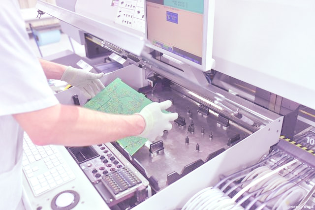
Unveiling the Cutting-Edge Technology of multilayer PCBs!
PCB boards, also known as printed circuit boards, are the carriers of electronic components and an essential element of circuits. They consist of substrates, conductive layers, printing layers, drilled holes, solder pads, and so on. The number of layers in a PCB board is an important factor that manufacturers and designers need to consider in the design and production process. In modern electronic products, multilayer PCBs are widely used.
How many layers can a PCB board have?
Firstly, it is important to understand that the number of layers in a PCB board refers to the number of conductive layers in the board, excluding non-conductive layers such as mechanical support, signal layers, and power layers. Commonly available PCB board layers include single-layer, double-layer, four-layer, six-layer, eight-layer, ten-layer, twelve-layer, etc. Generally, the more layers a PCB board has, the greater the manufacturing difficulty and cost. Therefore, the selection of a PCB board should be based on actual needs.
However, for special applications that require higher layer counts, such as integrating more electronic components on the same board or requiring higher signal transmission speed and lower signal interference, a multi-layer PCB board can be chosen. It is known that the highest number of layers for PCB boards available in the market can reach 60 layers or even more. However, manufacturing such PCB boards is highly challenging and costly, and they are typically used for special high-end applications.
In conclusion, the number of layers in a PCB board is determined by actual needs. In most cases, selecting a four-layer or six-layer PCB board is sufficient for the majority of applications. If a higher number of layers is required, factors such as manufacturing difficulty and cost need to be considered. Therefore, when choosing a PCB board, it is important to consider various factors and select the one that best suits the application’s needs.
On a theoretical level, multi-layer PCB boards can have any number of layers as long as the manufacturing equipment is capable. However, in practice, the most common PCB boards range from 4 to 10 layers, with special military or specific-purpose PCBs reaching over 100 layers. Nevertheless, these multilayer PCBs are not suitable for mass production.
Multilayer PCBs History
In 1961, Hazeltine Corp. from the United States introduced Multiplanar, which was the pioneer in multi-layer board development. This method is similar to the current manufacturing process of multi-layer boards using plated through holes. Since Japan entered this field in 1963, various conceptual designs and manufacturing methods for multi-layer boards have gradually become popular worldwide. As the transition from transistors to integrated circuits occurred and computer applications became more widespread, the demand for high functionality led to the focus on high wiring capacity and transmission characteristics in multi-layer boards.
Initially, three manufacturing methods for multi-layer boards, namely the gap method, the lamination method, and the plated through hole (PTH) method were introduced. The gap method was not practical due to its time-consuming manufacturing process and limited high-density capabilities. The lamination method, although offering high density, was complex and not as urgently needed at that time. However, as the demand for high-density circuit boards grew, the lamination method became a focal point for research and development by various manufacturers. Currently, the PTH method, which shares the same process as double-sided boards, remains the mainstream manufacturing method for multi-layer boards.
Contact Now


