PCB Design
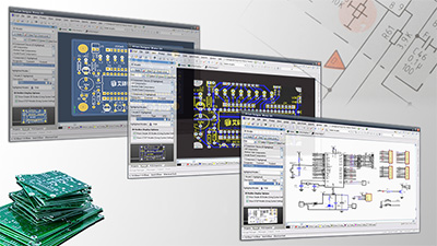
C-Alley has highly-skilled teams to find right solution for complex PCB design problems, Our teams of designers are qualified engineers with over 10 years of experience, also are experts of design through PADs PowerPCB, OrCAD, and more, C-Alley have designed many types of boards range from the consumer electronics, industrial, medical, and telecommunications industries, the design capability runs from small samples to large & complex circuit boards.
IPC class 2 and 3, JEDEC and MIL standards are available.
C-Alley PCB design as follows
- Single/double sided
- Multilayer; through via hole, blind/buried via and laser via technologies
- Flexible / flexi-rigid printed circuits
- HDI Designs with micro vias and advanced materials – Via-in-Pad, laser micro vias.
- High speed, multi layer digital PCB designs – Bus routing, differential pairs, matched lengths.
- PCB Designs for space, military, medical and commercial applications
- Extensive RF and analog design experience (printed antennas, guard rings , RF shields…)
- Signal integrity issues to meet your digital design needs (tuned traces, diff pairs…)
- PCB Layer management for signal integrity and impedance control
- DDR, DDR2, DDR3, DDR4, SAS and differential pair routing expertise
- High density SMT designs (BGA, uBGA, PCI, PCIE, CPCI…)
- Blind & Buried via ,Flex PCB designs, flexible rigid board of all types
- Low level analog PCB designs .
- Ultra low EMI designs for MRI applications
- Complete assembly drawings
- In-Circuit Test data generation (ICT)
- Drill, panel and cutout drawings design
- Professional fabrication documents creation
- Autorouting for dense PCB designs
PCB component placement and routing are carried out by experienced and committed designers to ensure an optimal layout for your high speed logic and high frequency RF boards.
C-Alley uses high frequency controlled impedance design methods, our team enables a fast autoroute service on complex designs like high density micro BGA boards.
Design Capability
| Design capability | Designed value | |
| Number of maximum design layers | 40 layers | |
| Number of maximum PINs | 60000 | |
| Minimum BGA space | 0.4mm | |
| Line width/line distance | 2mil/2mil(HDI) | |
| High-speed differential pair design | 2009 | 10Gbps,76cm |
| 2012 | 14Gbps,100cm | |
| 2013 | 28Gbps,10.6cm | |
Delivery capability
| Number of PINs for a single board | Delivery time of design(work day) |
| 0-1000 | 3-5 |
| 2000-3000 | 5-7 |
| 4000-5000 | 8-12 |
| 6000-7000 | 12-15 |
| 8000-9000 | 15-18 |
| 10000-13000 | 18-20 |
| 14000-15000 | 20-22 |
| 16000-20000 | 22-30 |
| Ultimate delivery capacity | 10,000pin/6days |


