DIP Assembly
It is common knowledge that producing high-quality printed circuit boards (PCBs) is a labor-intensive process that calls for extensive inspection, testing, mounting, and soldering. As a result, we provide full DIP assembly as one of our services. This aim to cut costs, improve accuracy and productivity, and make the whole process of assembling and checking PCBs from start to finish easier and faster.
DIP is the abbreviation for dual in-line package, also known as DIL package, and THT is the abbreviation for through-hole technology. In the PCBA industry, DIP assembly represents almost the same meaning as THT assembly and is a kind of electronic device package that consists of a rectangular enclosure and two parallel rows of electrical connection pins.
This type of PCB assembly refers to the process of mass-producing solder connections in which a printed circuit board (PCB) with components already installed is immersed in a tin furnace. All of the pins are parallel, point down, and stick out past the bottom plane of the package, at least far enough to be through-hole mounted to a printed circuit board (PCB), which means they can go through holes on the PCB and be soldered on the other side. The term “DIP” refers to a device packed as a plug-in, and the number of pins on this kind of device often does not exceed 100. Soldering DIP-packed components after surface mount technology (SMT) is a process often referred to as “DIP welding” or “DIP post welding.”
Why choose C-Alley Technology’s Electronics DIP Assembly?
C-alley provides DIP assembly (Dual In-line Package) service for various through hole components, i.e. DIP IC series, DO series, TO series power devices.All of our facilities and equipments are mainly for lead-free RoHS process. Our well trained personnel force on the production line, logical process flow & SOP, as well as stringent Quality Inspection are the fundamental assurance of our DIP production quality.
C-Alley technology has been serving the electronic industry for many years and has a wealth of knowledge in DIP processing. As the best turnkey through hole PCB assembly service company in China, we have served many projects in the welding machine and energy industry as well as the power control industry. The common theme of these projects is that the proportion of DIP processing on PCBA is relatively large. If you have specific demands for your printed circuit boards (PCBs), our process engineers are available to discuss DIP assembly technology in-depth. We guarantee on-time deliveries and, most importantly, the best possible customer service. DIP plug-in is an important part of the PCB assembly process and the quality of the DIP plug-in determines the quality of the PCBA processing. Next, let us show you our capabilities:
DIP Assembly Scale
- Full facilities from through-hole PCB fabrication to THT assembly;
- Comprehensive circuit board component procurement including SMD components, DIP components, integrated circuits, etc.
- Multiple testing guarantee services: manual testing, AOI testing, X-RAY testing, aging testing, flying probe testing, etc.
- 7 fully automatic through-hole assembly lines (including plug-ins, repairs, hand soldering wires and lead-free solder pots, etc.) that can mass
- produce 25,000 pieces of DIP ordinary products per month (minimum);
- In addition to quality control, C-Alley Technology also pays attention to staff training, and currently has 300+ professional production staff;
- Coexistence of manual through hole assembly and automatic DIP assembly;
- Ceramic Dual In-line Package (CERDIP or CDIP)
- Plastic Dual In-line Package (PDIP)
- Shrink Plastic Dual In-line Package (SPDIP)
- Kinny Dual In-line Package (SDIP or SPDIP)
THT Assembly Quality Assurance
- Strictly control the DIP pass-through rate;
- Workers with strict training, to control Productivity and quality;
- Strict IPQC and QA LOT sampling standards to ensure the reliability of THT processing;
- Before the plug-in, checks are done on the surface cleanliness of electronic components to detect oil stains, paint and other problems;
- During the plug-in, it can ensure that the electronic components are closed on the PCB to avoid unevenness and to uncover soldering pads well;
- If there is a direct indication on the surface of electronic components, we make sure insertion in the correct direction;
- Attention to the power strength of the plug-in components and to the PCB to avoid any damage due to excessive strength;
- Electronic components are not beyond the edge of any PCB board/frame, and we pay attention to the height and spacing between electronic components.
DIP PCB Assembly Service Process
Article Inspection
We first check and write down the quantity, item number, size, DIP component silkscreen number, value, etc., of all the parts you send us.
DIP Components Outline
Some component outlines need to be done ahead of time because of how they are made or because of the requirements for PCB DIP soldering and the whole PCB plan.
Through-hole component insertion
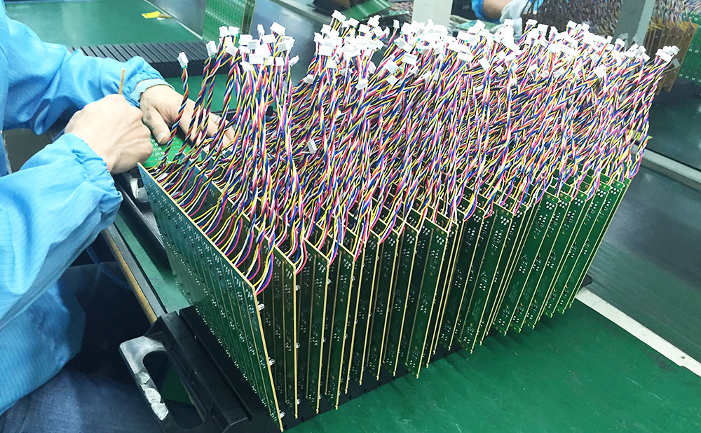
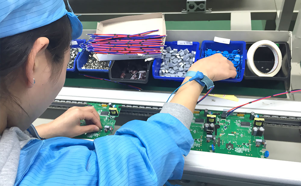
In this step, we place the material for the plug into the pins and then insert the pins into the PCB board. During plugging-in, it is essential to pay attention to the strength of the plug-in to prevent any damage to the circuit board or the nearby components. At the same time, we make sure that the PCB component orientation, component position, and component height are all consistent with one another.
Wave Soldering
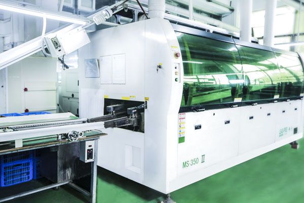
Nowadays, PCB assembly factories usually process the circuit boards after DIP through hole assembly by wave soldering. In wave soldering, flux is applied to a printed circuit board (PCB) during an in-line procedure. Then the printed circuit board is preheated before being submerged in molten solder.
The procedure of DIP wave soldering is done automatically. Having said all of that, the process starts with a PCB board which continues to travel ahead beside the conveyor belt.
After this, a machine sprays the board in a separate tank. At this point, a very thin coating of flux will be applied to the underlying surface of the PCB and its pins. After that, the board plate will go down to a zone where preheating.
In this region where the board covered in flux, the solvent begins to evaporate. Then, the active agent and the resin present in the PCB flux will undergo a process of decomposition and activation. During this step, you must give the board and the components complete preheating.
The bottom of the board encounters its first wave of molten solder as the board continues to move ahead. The welding flux is printed on the PCB with the assistance of this wave. The second wave of hot solder then strikes the bottom of the printed circuit board (PCB).
This moderate wave contributes to the division of the connecting bridge that is between the welding end and the pin. In addition to this, it eliminates welding faults.
There is a wide variety of solder machines on the market. Let’s briefly take a look at the machines!
A soldering machine typically has the following four components:
- Flux sprayer
- Preheating pad
- The pump creates the wave
- Pan solder
A wave soldering machine has a solder tank and a specific temperature will continue for the soldering process.
Most of the time, a solder wave is inside the tank and the PCBs will go over the bottom of the board. This means that the board links up with the solder wave at that point.
Additionally, one needs to be careful when changing the wave’s height. By doing this, you would have to stop the wave from going over the front of the board. This is when the solder gets to and where it needs to be.
The metal fingers on the conveyor make sure that the PCB stays in place in a specific spot. Different temperatures won’t hurt the metal fingers as it is made of titanium. Plus, the solder doesn’t change it in any way.
Manual Soldering of Components
Manual soldering is a traditional method of soldering leaded components to a PCB. It is generally suitable for small batch PCB assembly, laboratory assembly work, rework/repair, and the addition of extra components on a machine soldered assembly.
Part-to-part spacing
Manually soldered components should be placed further away from other components to avoid solder bridging. Typically, 50 to 100 mil pad-to-pad spacing should be maintained.
In the majority of instances, solder play an role as flux-cored wire. When producing soldered connections manually, the operator may see the creation of the junction and adjust the soldering process to different circumstances, such as solderability. With this in mind, manual soldering is still employed to make electrical connections that need the greatest level of dependability. However, when bulk soldering in need, manual soldering of high quality is not economically practical.
Use of Solder Iron
Learning to solder by hand is an acquired talent. An electrical current is utilized to heat the tip of the soldering iron. A soldering bit is a metal piece with a tinned tip used for soldering. Since heat conduction from the tip to the joints is generally weak, the tip temperature must be greater than the soldering temperature.
A soldering iron with a properly tinned tip is essential for achieving quality connections. Only a damp cloth or sponge, never a file or steel brush, should be used for cleaning. Commercially available soldering iron bits come in a wide range of shapes and sizes, with some being explicitly designed as hollow suction desoldering iron bits. Many have advocated for the tips to be standardized, although this has yet to happen.
Board Washing
The surface of the PCBA will still have flux, ionic impurities, organic residues, and other substances after the soldering process is complete. The majority of circuit leakage may be attributed to the impurities that have attached themselves to the surface of the PCBA board. These compounds have the potential to cause harm to electronic components and disrupt circuits. Ionic contaminants on the board’s surface can cause it to malfunction if kept in a humid environment. This will lead to common PCBA failures or even circuit board shorts. Because of this, not only is it necessary for us to clean the PCB before soldering but also the cleaning that occurs after soldering is of utmost significance.
Even though water washing is one of the more affordable options, it is often used only after an in-depth investigation of technical procedures has been conducted. Water-washing fluxes must be powerful enough to leave behind corrosive residues on the PCB and its components if used. It’s essential to keep in mind that water won’t remove rosin-based or synthetic, water-insoluble fluxes. Although water cleaning is a cost-effective option, it requires a thorough understanding of the underlying technology before it can be used effectively.
Cleaning the PCBA board can be used as one of the criteria to measure the strength of a through hole PCB assembly factory. As far as I know, many small workshops do not wash the board after the through-hole assembly completion, which may eventually lead to a rather ordinary inspection of the product by a customer although problems may arise when it is put into electronic applications.
Inspection and Functionality Test
During the through hole assembly process, your printed circuit board (PCB) must undergo several checks and the PCB assembly inspection process includes: visual inspections, AOI inspection, in-circuit testing (ICT) or flying probe tests, and even automated or semi-automatic bench tests. Printed circuit board (PCB) functional testing determines if we will send a produced board to a customer after it has been made and left the factory. PCB functional testing is the most exhaustive testing regimen available. The objective is to uncover manufacturing faults that impair dependability, such as missing or wrong components, and solder that isn’t correctly in connection.
This all means that the DIP PCBA board depends on incoming inspections that comply with the applicable standard and regulations. Things that need to be checked when inspecting components include whether the components’ performance, specifications, and packaging meet order requirements, product reliability requirements, assembly technology and equipment requirements, and storage requirements. In addition to the basic checks mentioned above, we also test the lead collinearity and lead coating layer thickness to verify that they can withstand heating and comply with the technology’s requirements.
Completed Product
After ensuring that there are no issues, the printed circuit board assembly (PCBA) will be put together with the housing, put through further testing, and ultimately sent. The creation of PCBAs is a loop of a ring, and since any fault in one link would substantially influence the quality of the product as a whole, strict control of each step is essential.
As a PCB assembly company, C-Alley Technology has spent a lot of time honing its expertise in DIP assembly. We are a one-stop shop for DIP assembly, electronic component procurement, finished product assembly, and testing.
In addition to implementing overall quality and environmental management, we also use cutting-edge machinery for PCB manufacturing and testing.
Manual or automatic through hole PCB assembly?
Automated through-hole Assembly
In THT automated assembly, machines that are controlled by a computer are used to position components on a circuit board. We may accomplish this by using various methods, such as machines to arrange components on the board or by using machines to solder the components into place. Using equipment, C-Alley technology ensures the best quality product assembly at the lowest feasible cost. Scheduled preventative maintenance is adopted to keep all of C-Alley technology’s machinery in good working order. Here are the advantages of choosing our automated DIP assembly services:
- Fully automatic equipment can easily achieve fast turnaround PCB assembly, and it is more suitable for high-volume PCB assembly. The assembly method is ideal for swiftly constructing a large number of PCBA or creating anything that is highly complex and has a lot of DIP components;
- Automated assembly may help you save both time and money while producing products of a high standard. Compared to manual assembly, automated thru-hole assembly offers a variety of benefits that may make it the superior option;
- The primary advantage is that machines position components considerably more rapidly than a person can. In addition to this, the method is versatile enough to deal with boards of varying dimensions and degrees of complexity.
Manual through-hole Assembly
When it comes to complex DIP assembly tasks, C-Alley is up to the task. We’ve structured our manual lines to cut down on product movement and worker motion as much as possible. The accurate and complete assembly is guaranteed by careful documentation and in-process inspections. We are a versatile and reasonably priced contract manufacturer because of our DIP assembly expertise. Manual printed circuit board DIP assembly inspection starts with using a microscope, so it is slower and suitable for small batch PCB assembly orders. Here’s why through-hole assembly has survived:
- Low-volume orders, especially those involving very tiny or fragile components, sometimes need this assembly;
- There is a high degree of accuracy, and the user may readily adjust the positioning of each part. However, it is time-consuming, costly, and challenging to master;
- Assembling by hand provides greater room for personalization and adaptation. When using automated DIP assembly, you can only work with the components the machine offers;
- Assembling components by hand also encourages greater originality and improvisation. You may be creative in your approach to PCB assembly without being limited by mechanical means. This might result in increased product quality and a more significant advantage in the market;
- Power outages and other environmental factors may have a negative impact on automated assembly, leading to faulty products. Manual assembly is immune to delays like this. You may exert greater influence on the final result.
Conclusion
The PCBA electronic processing industry continues to rely heavily on DIP for various reasons, making it a vital component. In contrast to the SMT plug-in, which is automated, the DIP plug-in calls for a large-scale manual process that takes a significant amount of human effort. Due to the extensive labor percentage, the failure rate of DIP assembly is considerable. As a result, keeping an eye on the quality of the PCBA when performing DIP processing is essential. DIP is the follow-up work of SMT, an important part of the PCB assembly process. However, large-sized components cannot be inserted by the auto machine, but manually plugged in, and then passed through the reflow oven to finally be soldered.


