Flex and Rigid-flex Layer Startup Types

FLEX AND RIGID-FLEX LAYER STACKUP TYPES

There are a number of standard stackups available for flex and rigid-flex circuits, referred to as Types. These are summarized below.


Type 1 – Single Layer

Single-sided flexible wiring containing one conductive layer and one or two polyimide outer cover layers.

  • One conductive layer, either laminated between two insulating layers or uncovered on one side.
  • Access holes to conductors can be on either one or both sides.
  • No plating in component holes.
  • Components, stiffeners, pins and connectors can be used.
  • Suitable for static and dynamic flex applications.


A Type 1 flex structure with 2 cover layers, access holes on both sides and no plating in the in the component holes.


Type 2 – Double Layer

Double-sided flexible printed wiring containing two conductive layers with plated through holes, with or without stiffeners.

  • Two conductive layers with an insulating layer between; outer layers can have covers or exposed pads.
  • Plated through-holes provide connection between layers.
  • Access holes or exposed pads without covers can be on either or both sides; vias can be covered on both sides.
  • Components, stiffeners, pins and connectors can be used.
  • Suitable for static and dynamic flex applications.


A Type 2 flex structure with access holes on both sides and plated through holes.


Type 3 – Multilayer

Multilayer flexible printed wiring containing three or more conductive layers with plated-through holes, with or without stiffeners.

  • Three or more flexible conductive layers with flexible insulating layers between each one; outer layers can have covers or exposed pads.
  • Plated through-holes provide connection between layers.
  • Access holes or exposed pads without covers can be on either or both sides.
  • Vias can be blind or buried.
  • Components, stiffeners, pins and connectors can be used.
  • Typically used for static flex applications.


A Type 3 flex structure with access holes on both sides and plated through holes.


Type 4 – Multilayer Rigid-Flex

Multilayer rigid and flexible material combinations (Rigid-Flex) containing three or more conductive layers with plated-through holes. Rigid-flex has conductors on the rigid layers, which differentiates it from multilayer circuits with stiffeners.

  • Two or more conductive layers with either flexible or rigid insulation material as insulators between each one; outer layers can have covers or exposed pads.
  • Plated through-holes extend through both rigid and flexible layers (apart from blind and buried vias).
  • Access holes or exposed pads without covers can be on either or both sides.
  • Vias or interconnects can be fully covered for maximum insulation.
  • Components, stiffeners, pins, connectors, heat sinks, and mounting brackets can be used.


A Type 4 rigid-flex structure, the rigid sections are formed by adding rigid layers to the outside of the flex structure.

Rigid-flex Circuit Boards Design

Rigid-Flex circuit boards Design

Flexible circuit board technology was initially developed for the space program to save space and weight. They are popular today as they not only save space and weight – making them ideal for portable devices such as mobile phones and tablets – they can also: reduce packaging complexity by substantially reducing the need for interconnect wiring; improve product reliability due to reduced interconnection hardware and improved assembly yields; and reduce cost, when considered as part of the overall product manufacture and assembly costs.

The biggest problem with designing rigid-flex hybrid PCBs is making sure everything will fold in the right way while maintaining good flex-circuit stability and lifespan. The next big problem to solve is the conveyance of the design to a fabricator who will clearly understand the design intent and therefore produce exactly what the designer/engineer intended.

Rigid-Flex circuit boards require additional cutting and lamination stages, and more exotic materials in manufacturing, and therefore the cost of re-spins and failures are very much higher than traditional rigid boards. To reduce the risk and costs associated with rigid-flex design and prototyping, it is desirable to model the flexible parts of the circuit in 3D CAD to ensure correct form and fit. In addition, it is necessary to provide absolutely clear documentation for manufacturing to the fabrication and assembly houses.

C-Alley engineering team offers full flex and rigid-flex circuit boards design services. During our application review and quoting process, we carefully examined specifications, materials, and construction in order to minimize and eliminate any technical issues.

We also look for areas of opportunity for improving the design of your flex or rigid-flex circuit’s reliability, and functionality. Cost reductions are also identified to generate an accurate quote that is based on a manufacturable, reliable, and cost-effective design.

2017’s effect that Trump will make on electronics manufacturing?

2017’s effect that Trump will make on electronics manufacturing?

I think it’s very interesting but important topic to discuss about the breaking year and possible changes.

What could a Trump effect look like in 2017? I think there are several positives:

A president who is pro-manufacturing. We haven’t had a champion of manufacturing in the White House in a long time … decades, in fact. Having a president who understands we need transformative manufacturing jobs to stay globally competitive is a huge win for manufacturing companies. More important, having that message frequently repeated will help counter the myth that US manufacturing is no longer a viable career path.

A president who understands the impact of taxation and regulation on business growth. Taxation and regulation is strangling mid-size businesses and incentivizing businesses that move offshore to do so. Reversing that will incentivize more US investment. China originally gave five-year tax holidays to attract the electronics industry. It worked pretty well.

A president favoring revisions to the Affordable Care Act. ACA is a huge cost to both companies and individuals that are not receiving subsidies. Increased competitiveness in insurance options and more cost transparency would be welcomed by most businesses.

A president who isn’t afraid of nationalism. I have yet to visit a country other than the US that sees nationalism as a dirty word. Most developed nations find ways to put the interests of their citizens before the interests of the global community. They recognize employed workers earning a market-driven living wage costs taxpayers less money. Having a president cheerlead a Buy USA movement will benefit US manufacturing.

But what about the scary side?

The impending trade war. If President Trump enacted all the promises he made on the campaign trail, we might have a trade war. However, I think his behavior suggests he is simply setting a hard tone to improve negotiations and put the US in more favorable positions. Many of our trade deals are bad, and we routinely ignore unfair trade practices. Long term, having a fair trade focus will benefit US companies. Short term, companies with operations in parts of the world that benefit from our weak trade deals may see retaliatory practices in those countries.

The border wall and NAFTA. US and Mexico business is intertwined significantly. Finding the right way to balance our immigration regulation with Mexico’s desire to further its national interests will be challenging. As I write this, the Mexican peso has devalued to 21 pesos to the dollar. I can’t help but believe some of that is due to a desire to make Mexican manufacturing costs look even more attractive. A strong manufacturing base in Mexico may help bring back the supply-chain advantage lost when large-scale manufacturing migrated to China, which is a positive. However, that level of devaluation can create instability and ultimately impacts the ability of Mexican nationals to buy US goods and services. It also creates issues for companies whose expenses are paid in both pesos and dollars. Tighter immigration enforcement combined with reforms that make it easier for economic immigrants who don’t want citizenship to work here will help US businesses that play by our immigration rules and cut down on worker exploitation on this side of the border. Achieving the right balance in trade, immigration and security won’t be easy, but is critical to both countries’ interests.

Shaming government contractors. As a taxpayer I like the idea of someone asking hard questions about cost overruns. As a business owner I realize the pitfalls, particularly when being called on President Trump’s carpet drops stock prices. Hopefully this is also an area where better balance is found on both sides. From the EMS perspective, expect more pressure to cut costs.

China and Russia. We can’t live peacefully in a world where we don’t have shared strategic interests with these two countries. However, we also can’t live peacefully in a world where either of these countries holds all the cards. It will be interesting to see how President Trump addresses this, since China still holds a lot of good cards and Putin bluffs well.

SMT Package Technology:BGA and QFN

Assembly BGA / QFN / SMT PCB Board

Manufacturer of a BGA / QFN / SMT PCB assembly board with ENIG/HASL surface finish, rework stations, reflow soldering equipment, reflow ovens, and smt pick and place machines. our engineering experience and commitment to excellence have earned us the reputation in Europe, Russia, USA, Canada, Australia.

C-Alley offers professional rework, repair and prototype builds of PCBs. Our experienced instructors teach professional soldering classes as we are an IPC certified training center.

C-Alley designs and manufacturers innovative equipment for assembly, soldering, and rework of printed circuit boards and hybrid microelectronics.  Our product line consists of BGA Rework Stations, Reflow Ovens, and SMT Pick & Place Systems ideal for environments with prototype to medium volumes.

For over 10 years we have built a solid reputation based on delivering quality products that not only perform to specifications but also exceed customer expectations.  C-Alley has made PCB board with a wide range of industries incluing: aerospace, consumer electronics, contract electronic manufacturing, government, industrial OEM’s, medical, military, semiconductor, telecommunications, and universities.  More than 500 of our products have been installed worldwide.

PCB Assembly Equipments

PCB assembly equipments

C-Alley is a leading manufacturers of PCB assembly & design,  soldering, and rework , it’s equipped with SMT Pick & Place machines , BGA rework stations, reflow ovens for prototyping to medium volumes, all services of assembly, cleaning ,inspection, dipping conformal coat, repair we would like to offer.

A professional SMT equipment manufacturer providing worldwide sales, service and spare parts.

C-Alley is a one-stop SMT solution company, providing all SMT production, inspection and rework machines, spare-parts, consumables etc.

Product line includes: pick and place systems, reflow ovens, wave soldering equipment,screen printers, stencil printers,PCB conveyors and PCB handling equipment, AOI, SPI, conformal coating machines, dispensers,selective soldering equipment, PCB cleaners. Also, we provide replacement parts likeconveyor fingers for different wave solder systems, pick and place feeders and nozzles,consumable materials like glues, solder wire etc.

Quality check: For all systems shipped to customer’s sites, certification and compliance has been completed by International Compliance Consultants for each machine released by our team. Plus QC checking will cover safety, electrical, mechanical, functionality, cleanness and packing. All machines need to pass through an aging time process, which will simulate working conditions at a customer site.

Machine record database: A database of all installed machines is established, ensuring trace-ability of all component versions. It will cover a machine’s configuration and parts used in the machine. This will maintain our ability to support customers, for many years after the machine has been replaced.

Machine Documentation: Full Specifications, installation, operational and any software detailed  manuals, operational videos, sales support videos and presentations for each machine, are available. All provided in English.

Financial support: We are working with HSBC bank and local banks to provide a LC service, when the order amount is over certain value. This means if a customer has a good reputation at their bank, they can order, take delivery and go into production without any down payments.

Installation and after sale service: All supporting technical engineers graduated from Electronic & Mechanical departments of Universities, they have good English. They have been fully trained at manufactures sites, so on-site installation and training for each system is available, if required.

PCB Layout to design process

PCB Layout to design process

PCB design equipment
In the early days of PCBs, the design and layout was undertaken manually using tape that was placed onto a translucent film. These PCB designs were normally four times the required size and they were photographically reduced onto a 1:1 film for the PCB production process.
Nowadays the PCB design process has been computerised and there are many PCB CAD systems and PCB software packages that enable the PCB layout and design to be undertaken more efficiently than before. The PCB software varies considerably in price. Budget, or even free software provides the basic functions, whereas the top end packages enable many more facilities to be incorporated into the design. Simulations, complex routing, and many more facilities are available.
Circuit schematic capture
The first stage in the development of a PCB design is to capture the schematic for the circuit. This may be achieved in a variety of ways. Circuits may be entered into a schematic capture tool. This may form part of the PCB design suite, or it may be an external package whose output can be exported in a suitable format.
In addition to purely performing the schematic capture, simulations of the circuit may be undertaken at this stage. Some packages may be able to interface to simulation packages. For applications such as RF circuit design simulation of the circuit will enable the final circuit to be optimised more without building a prototype.
With the schematic capture complete the electronic design of the circuit is contained within the file and can be converted to what is termed a “netlist”. The netlist is the interconnectivity information and it essentially the component pins and the circuit nodes, or nets, to which each pin connects.
PCB component placement
Before proceeding with the detailed PCB design and layout, it is necessary to gain a rough idea of where components will be located and whether there is sufficient space on the board to contain all the required circuitry. This will enable decisions about the number of layers needed in the board, and also whether there is sufficient space to contain all the circuitry may need to be made.
Once a rough estimate has been made of the space and approximate locations of the components, a more detailed component layout can be made for the PCB design. This can take into account aspects such as the proximity of devices that may need to communicate with each other, and other information pertaining to any RF considerations for example.
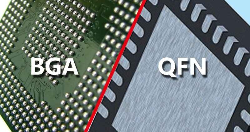
In order that components can be incorporated into the PCB design they must have all the relevant information associated with them. This will include the footprint for the printed circuit board pads, any drilling information, keep out areas and the like. Typically several devices may share the same footprint, so this information does not have to be entered for each component part number. However a library for all the devices used will be built up within the PCB layout design system. In this way components that have been used previously can be called up easily.
Routing
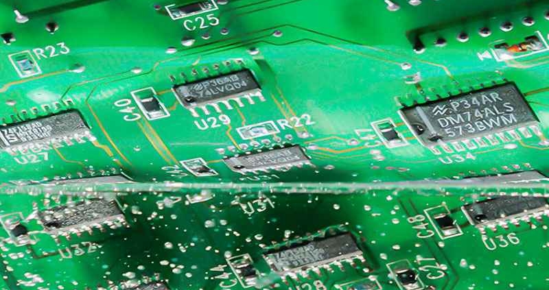
Once the basic placement has been completed, the next stage of the PCB design is to route the connections between all the components. The PCB software then routes the physical connections on the board according to the netlist from the schematic. To achieve this it will use the number of layers that are available for connections, creating via holes as required. Often one layer will be allocated for use as a ground plane, and another as a power plane. Not only does this reduce the level of noise, but it enables low source resistance connections to be made for the power.
The routing can use a significant amount of computing power. This is particularly true for larger designs where there may be upwards of three or four thousand components. Where routing is difficult as a result of high component density, this can result in the routing taking a significant amount of time.
PCB files
The information for the photo plots of the PCB layout are outputted in the form of Gerber files. This format is the standard for PCB files and they are a form of numerical control file that is used by a photo plotter. In addition to the Gerber files, drill information is also generated along with the screen print and photo-resist information.
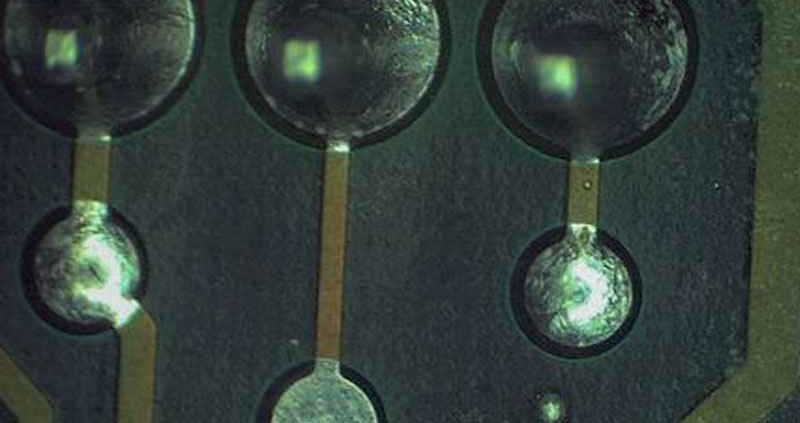
One major element in the cost of a printed circuit board is the drilling. In any design some holes are required for fixing as well as those required for any conventional components needed. However to reduce costs it is wise to use as few hole sizes as possible. In this way the drill will need changing less and time can be reduced.
PCB overview
Once complete the information for the PCB will be used in many areas of the manufacturing process. Not only will it be used for the manufacture of the actual PCB itself, but the files will also be used in other areas of the manufacturing process. They may be used to develop a pick and place programme, and in addition to this the files may be used in the manufacture of a PCB solder mask for adding solder paste to the board prior to component placement. The files may also be used for developing various forms of test programme such as an “In-Circuit Test” (ICT), and particularly in developing any bed of nails test fixture. In this way, the PCB design is a crucial element of the whole manufacturing process for any product. The PCB design is more than just a design for the basic board.
C-Alley, a China manufacturer of SMT and PCB assembly equipment, was awarded an order to design, build and commission a unique reel-to-reel in-line PCB assembly line. The customer, a large international medical & smart home, automotive, PCB assembly systems products, C-Alley is a leading China manufacturer of OEM equipment for the short to medium run production environment.
PCB Surface Finish & Conformal Coating

PCB Surface Finish & Conformal Coating

HASL /Electroless Nickel Immersion Gold (ENIG)

Refer to past projects, the most popular surface finish choices of customer is HASL,as its low cost and robust, fundamental changes in the PCB industry—namely, the rise complex surface mount technology—have exposed its shortcomings. HASL leaves uneven surfaces and is not suitable for fine pitch components. Although it does come in lead-free, there are other lead-free options which will likely make more sense for a high-reliability product.

ENIG is quickly becoming the most popular surface finish in the industry. It’s a double layer metallic coating, with nickel acting as both a barrier to the copper and a surface to which components are soldered. A layer of gold protects the nickel during storage.  ENIG is an answer to major industry trends such as lead-free requirements and rise of complex surface components (especially BGAs and flip chips), which require flat surfaces. But ENIG can be expensive, and at times can result in what is commonly known as “black pad syndrome,” a buildup of phosphorous between the gold and nickel layers that can result in fractured surfaces and faulty connections.

Recently the cases to dip conformal coating are more popular, conformal coatings protect your electronic printed circuit boards from moisture and contaminants, preventing short circuits and corrosion of conductors and solder joints.

They also minimize dendritic growth and the electro-migration of metal between conductors.

In addition,conformal coatings protect your circuits and components from abrasion and solvents. Stress-relieving is also provided, as well as protection of the insulation resistance of the circuit board.


Solder balls and solder beading problems

Solder balls and solder beading have been a process issue for many years and they may not cause product failure or quality problems but they are not desirable. Solder balls are caused by a variety of factors in different processes and should be resolved to eliminate a poorly defined process or a process and materials which are out of control .

Solder beading is a special phenomenon of solder balling when using solder paste in certain SMT applications. In brief, solder beads are large solder balls near components with very low stand-off . With more attention being drawn to no-clean paste applications due to CFC concerns, a better understanding of this event becomes indispensable.

Solder balling can be caused by poor process conditions with gassing from the flux during wave contact or excessive turbulence as the solder flows back into the bath which causes spitting. Solder balls can be ejected from the joint area during soldering due to excessive outgassing of the PCB.

So way you can remedy this by modifying your aperture, and hence your print shape, of the solder paste deposit for those ceramic capacitors.

Constraints for PCB Design

Creating constraints for a PCB design

C-Alley provides PCB design , PCB Fabrication, PCB Assembly services , with advanced SMT line equipment, ovens, pick & place systems, X-ray and AOI systems, will improves accuracy, productivity and efficiency in a highly reliable, compact unit.

Are your constraints constraining you? Creating constraints for a PCB design can ensure necessary rules are followed during placement, fanout and routing. Defining constraints for items like component-to-component spacing, trace-to-trace, etc. through all types of signal integrity rules is all-important to ensure the PCB is functional and can be fabricated and tested. So, can a PCB design be over-constrained? If so, what issues does it create for the designer, and subsequently, is it possible to orchestrate and apply design constraints in such a way that the design does not get bogged down?

Overly constrained designs can contribute to missing critical deadlines. Two important things to consider with constraints are constrain only what must be constrained, and have a PCB design strategy that ensures the job is completed on time. Things like optimized placement and knowing how and when to execute component fanouts are key. Take advantage of components that have pin, gate or even package swapping. Testing different routing strategies and executing interactive and autorouting such that you optimize routing channels can help ensure PCB design success.

Designing and manufacturing electronic boards

Designing and manufacturing electronic boards

If you prototype printed circuit boards , how can you ensure that laminates and prepregs you used will match those used in offshore volume production?

As an industry, those of us involved in designing and manufacturing electronic products can all agree that we now live and operate in a global supply chain environment. Since a lot of what is incorporated into current and next generation products is reflected in the software, this isn’t much of a concern. Take your favorite products, download the latest software update and newly developed apps and you’re ready to go.

When it comes to developing the pieces of hardware, the process is not so simple. And, when it comes to printed circuit board (PCB) development efforts, the process becomes even more challenging. That’s because PCBs are the launching points for hardware product development and the laminate and prepreg materials used in designing and manufacturing PCBs are the nuclei for those boards. (Prepreg is fiberglass cloth that has been saturated with resin that is not fully cured. As a PCB is placed under the heat and pressure of lamination this resin melts and flows into the voids in the adjacent copper layers filling them.)

  • Gerber data, which board and stencil manufacturers still depend on for their processes. There will be a point when this is not required. Depending on your vendor base, that time may or may not be now.
  • Valor ODB++, which  allows board and stencil manufacturers to gain insight into the design and offer feedback to improve processes, thus reducing production cost over time. It also allows use of Valor DFA software for reviewing an assembly to improve yields in production by PCB manufacturers with that level of sophistication. Since it can be used for programming pick-and-place lines, it could be a “one file” approach to all manufacturing requirements.
  • CAD ACSII database, which supports the fastest approach to programming the pick-and-place lines and can support other programming efforts such as AOI.
Sitemap | ©Copyright 2023 H.K C-Alley Co., LTD. | Alibaba | KingshengPCBA | All Rights Reserved