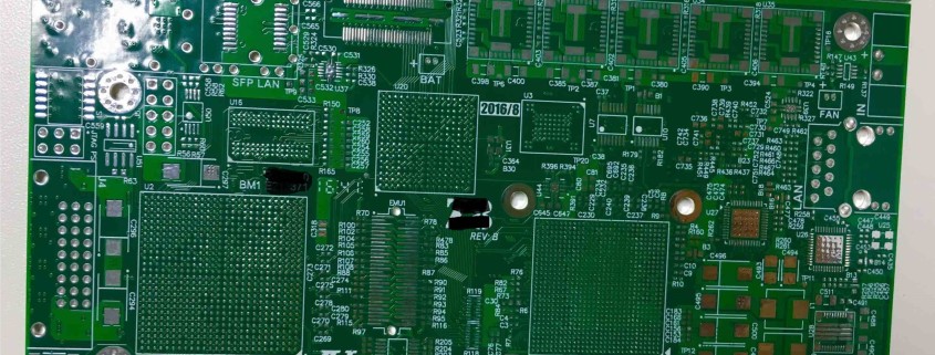
PCB Manufacturing Capabilities –advanced PCB Fabrication Equipments.
With over 10 years productin experience in PCB manufacturing , from Prototyping to finished board with components, also Box build assembly.
Welcome to send us an quote : [email protected]
Your inquiry will be replied within 24 Hrs .
HDI technology including Rigid and Flex-Rigid Printed Circuit Boards with blind vias, buried vias, blind micro-vias, copper filled micro-vias, resin filled vias, stacked vias, sequential build-up, buried resistance and buried capacitance.
- PCB Layout, CAD, Design for Manufacturability and Cost (DFx)
- Quick-turn PCB Prototyping for High Technology PCBs, Circuits
- High-volume, 100% electronical testing
- Advanced Technology: Latest Laminates, HDI, any Layer Via Structures, Multiple Sequential Laminations
|
|||||||
| Base Material Used | FR4 – FR4 HiTg° | BT Epoxy – Polyimide -Teflon – INVAR – Halogen Free – Hi Frequence | BT Epoxy – Polyimide -Teflon – INVAR – Halogen Free – Hi Frequence | ||||
| PCB Type | Rigid | Rigid – Rigid – Rigid/Flex (hybrid) | Rigid – Rigid – Rigid/Flex (hybrid) (Teflon+Kapton) |
||||
| Maximum Number of Layers | 16 | 36 – 32 – 24 | 40 – 40 – 32 | ||||
| Maximum Board Dimension | 570 x 449 | 640×570 mm | |||||
| Maximum Board Thickness | 3.2 mm | 6.5 mm | |||||
| Minimum core Thickness | 0.1 mm | 0.05 mm – 0.025 (Flex) | |||||
| Base Copper Thickness | 18 – 35 – 70 µ | 9-12-18-35-70-105-140-210-305 µ | |||||
| Aspect Ratio | 8:1 | 24:1 | 30:1 | ||||
| Minimum Diameter Hole (Mechanical) | 0.2 mm | 0.15 mm | 0.1 mm | ||||
| Minimum Diameter Hole (Laser) | 100 µ | 75 µ | 60 µ | ||||
| Nickel Thickness on the Connector | > 4 µ | > 4 µ | |||||
| Gold Thickness on the Connector | > 0.8 µ | > 0.8 µ | |||||
| Holes Position Tolerance | ± 0.1 mm (from the board edge) |
± 0.07 mm on PCB with diagonal < 300 mm (from the board edge) |
|||||
| Minimum Trace | 100 µ | 75 µ | 50 µ | ||||
| Minimum Space | 100 µ | 75 µ | 50 µ | ||||
| Plated Hole Tolerance | -0.05 ÷ + 0.1 mm | -0.05 ÷ + 0.05 mm | |||||
| Unplated Hole Tolerance | 0 ÷ + 0.1 mm | 0 ÷ + 0.1 mm | |||||
| Conformity Certificate | On demand | On demand | |||||
| Test Certificate | On all delivery | On all delivery | |||||
| Controlled Impedance Certification | On demand | On demand | |||||
| Production Date (week and year) | On solder mask On copper (on demand) | On solder mask On copper (on demand) | |||||
| Certification | UNI EN ISO 9001:2008 – ISO TS 16949-2002 UL Certified: 94V-0 up to 130° | UNI EN ISO 9001:2008 – CNES – AS9100B EN9100:2003/S1 – JISQ9100:2004 UL Certified: 94V-0 up to 130° |
ISO 14000 | ||||
| Routing Tolerance | ± 0.2 mm | ± 0.15 mm | |||||
| Surface Finishes | H.A.S.L. – Lead Free H.A.S.L. Electroless Gold Electroless Tin – OSP |
Electrolytic Ni – Electrolytic NiAu | |||||
| Solder Mask Types | Photographic | Photographic | |||||
| Legend | White | Different Colours | |||||
| Electrical Test (short and open) | 100.% | 100.% | |||||


