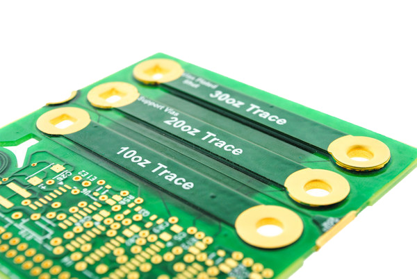
Tips for Designing Circuits
Minimum line width is one of the first questions asked of a PCB manufacturer’s capabilities, but the answer rarely includes “depending on copper weight.” To simplify your design process and avoid problems at the time of manufacturing, we will demonstrate how and why line width depends on copper weight. This brief overview gives some near-universal rules for trace width versus copper weight, along with other important tips when using heavy copper PCB.
Copper Weight and Trace Width
During etching, copper traces are only protected from the top by either a dry film or a tin plate, meaning that as copper is etched away, the sides of the trace are also etched (in other words, etching is an isotropic process). There are two main results of the isotropic etching – first, thick copper requires wider trace and space, and second, traces finish with a trapezoidal shape. Below are some current guidelines for trace width versus copper weight.
Copper Weight
| Starting Copper | Minimum Trace | Minimum Space |
| 0.5oz | 0.003″ | 0.003″ |
| 1oz | 0.005″ | 0.005″ |
| 2oz | 0.008″ | 0.008″ |
| 3oz | 0.012″ | 0.012″ |
| 4oz | 0.016″ | 0.016″ |
The table specifies starting copper and assumes the use of a pattern plating process, as is the case with the majority of PCBs. With rare exceptions, finished copper is one ounce greater than starting copper on the outer layers, while on inner layers, finished copper is the same as the starting copper.
By far, 1oz copper thickness is the most common and standard copper weight. This is because it often hits Goldie Lock’s sweet spot of not being too much or too little. 2oz copper thickness is often more than is required while costing considerably more, and 0.5oz copper may not be enough, especially for ground planes that must endure higher currents. Therefore, 1oz copper thickness if often the most ideal choice for fitting your design and budgetary needs.
What if you need tighter trace and space? Typically, you can duplicate the layer that requires heavy copper, then cut the copper weight in half. Therefore, if you need 8 mil lines and 4oz copper, duplicating the layer and using 2oz copper is the best alternative.
For starting copper weights of 5oz or greater, we also recommend doubling a layer as opposed to using thicker copper. The cost and processing difficulty of the thicker copper means that adding layers is cheaper than using the thick copper. In other words, a 2-layer, 6oz copper board is usually more expensive than a 4-layer, 3oz copper board.
Heavy Copper PCB Considerations
On the outer layers, there are two additional considerations for heavy copper. Sooner and simplest is a solder mask – when using liquid solder mask, multiple coats are required to adequately protect heavy copper traces. This problem is mitigated by 3D-printed solder masks, but that technology is not available at every facility or in every color.
Second, surface mount pads can be compromised by heavy copper. Your Gerber file specifies the trace width at the base of the trace, but SMT happens on the top of the trace. With heavy copper PCB, the top of the SMT pad may be several mils thinner than designed, leading to the more difficult placement and potentially a weaker solder joint.
Cross-Sectional Area of Traces and Vias
One of the most important calculations in high-current applications is the cross-sectional area of a trace. IPC 2152 shows (conservative) cross-sectional areas needed for particular amperages, but designers are left alone to calculate the area of a trapezoidal trace. Sure, the area of a trapezoid is h*(b1+b2)/2, h is obviously copper weight (in mils!) and b1 is obviously the trace width, but what is b2? Your PCB manufacturer’s sales and planning departments will know how much smaller the top of the trace is than the bottom, so be sure to ask them. Note that the difference varies from manufacturer to manufacturer.
The cross-sectional area of a via comes from knowing how much plating is in the via. With Class 2 plating, the via wall is 20 microns (0.0008”) thick. With Class 3 plating, the via wall is 25 microns (0.0010”) thick. Use these thicknesses and the diameter of your via to calculate the cross-sectional area of a via, keeping in mind that the cross-section makes an annulus. Note that Class 3 plating is commonly requested on Class 2 boards. Hole wall plating thicker than 25 microns is not difficult in low volumes but is not recommended for a production part. Duplicating vias is usually a better solution than overplaying. Using a conductive via fill helps only marginally. Via fill material is epoxy, meaning that the current carrying capacity is not as high as pure silver or copper.


