

• MOB:+86 19879928172
  • Email: chinapcba@c-alley.com
C-Alley
  • PCB
    • PCB Types
      • Multi-layer PCB
      • Flexible PCB
      • Rigid-flex PCB
      • HDI PCB
      • High Frequency PCB
      • Hybrid Laminates PCB
      • Metal Substrate PCB
      • PCB Fabrication
      • PCB Prototype
      • Quick Turn PCB
  • PCBA
    • PCB Assembly
      • PCBAs
      • Prototype PCB Assembly
      • SMT Assembly
      • BGA Assembly
      • DIP Assembly
      • Soldering Assembly
      • Box Build Assembly
    • Our Strength
      • Production Capability
      • PCBA Plant Equipment List
      • Quality Control System
      • Comprehensive Test
      • Parts Sourcing
      • Guarantee
      • Added Service
  • EMS
    • PCB Design
    • Schematics Diagram
    • PCB Layout
    • Electronics Reverse Engineering
    • Chip Decryption
    • PCBA Copy & Redesign
    • Customized Function
    • SI-PI-EMC Analysis
    • Mechanical Design
  • Applications
  • About Us
    • C-alley
    • Why us
    • Equipments
    • Visit us
  • News
  • Contact Us
  • Menu Menu

Testing Jig

The testing jig is important so we can spot errors in the PCB before sending it to the final assembly line.

The test jig has two functions:

1) to check that the preamp can hold voltages applied to the power rails and that the supply currents drawn are within tolerance

2) to provide a fast electronic pulse that is applied to the input of the preamp and compare the output waveform to an expected shape.  The tester is also designed to be operated conveniently and quickly.

At C-Alley, we do ofen customized test jig design and manufacturing. All the PCBA products must be 100% fully tested.
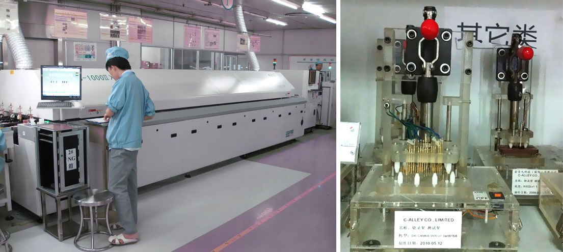
Testing Jig

Testing Jig

To facilitate the fabrication of a test jig, ECAD (Electronic Computer-Aided Design) files are required to automatically identify test points, mounting holes, and other test features. The supported file formats for test jig fabrication include:

  • Altium Test Point Reports (.csv)
  • Eagle (.brd)
  • Gerbers (.zip)
  • KiCAD (.kicad_pcb)

When designing the test jig, you can select the appropriate test probe card and receptacle types from a list of compatible parts. You can add, modify, or remove probes and guide pins as needed. Additionally, you can configure the location of the Device Under Test (DUT) and panelization settings to allow for testing an entire panel at once. It is recommended to visually review the generated jig before finalizing the design.

For test jig fabrication, you can download the Design File Package, which includes all the necessary files to build the fixture. These files can be used for fabricating the plates using methods such as acrylic fabrication, CNC milling, or laser cutting.

During the test jig assembly process, you should attach all the probes and guide pins, integrate your test instrumentation, and proceed with running your tests.

In terms of Design for Test (DFT), it is important to consider the following tips to make testing your PCB assemblies easier when using a bed-of-nails style test fixture:

  • Place all test points on a single-sided PCB, preferably the side with fewer components. This helps reduce the cost and complexity of the test fixture required for testing the PCB in both rigid and flexible forms.

By following these guidelines and considering DFT principles, you can streamline the test jig fabrication process and enhance the ease of testing your PCB assemblies.

  • arrow PCB Fabrication
  • arrow PCB Prototype
  • arrow PCB Categories
  • arrow Quick Turn PCB

Send Us Enquiry

    Latest News

    • PCBA SMT processing lead timePCBA SMT processing lead timeOctober 13, 2023 - 7:59 am
    • PCBA Applied in Electronic ProductsPCBA Applied in Electronic ProductsOctober 13, 2023 - 6:12 am
    • PCB Assembly approachesThree Approaches to Ensure PCBA Assembly Service CompletedJuly 29, 2023 - 10:12 am
    • Precautions in the Process of Prototype PCB ManufacturingJuly 25, 2023 - 8:25 am
    • 2023 China PCB marketGlobal and China Printed Circuit Board (pcb) Market Survey 2023July 14, 2023 - 7:21 am
    • Multilayer PCBs Versus Double-sided PCBsThe Key to High-Performance: Double-sided PCBs to Multi-layer PCBsJuly 12, 2023 - 4:14 am

    About C-alley

    C-Alley (H.K.) Co.,LTD is a tailored and professional One-stop PCBA and EMS service company in China, we have been helping customers with Innovations for electronic design services for over 13 years. We are dedicated to meeting the demands of our customers.

    Addr: 2/F, Building 6, Tangtou 3rd Industrial Zone, Tangtou Community, Shiyan Town, Baoan District, Shenzhen, China, 518108
    Email: chinapcba@c-alley.com
    Tel: 86-755-27202654
    Skype: kingsheng.pcba10

    Capabilities

    • PCB Design
    • PCB Fabrication
    • PCB Prototype
    • Multilayer Rigid PCB
    • Flexible PCB
    • Rigid-flex PCB
    • HDI PCB
    • High Frequency PCB
    • Hybrid Laminates PCB
    • Metal Substrate PCB
    • Prototype PCB Assembly
    • PCBA Test

    Certifcates

    PCB ISO Certificate PCB CE Certificate PCB ROHS Certificate PCB UL Certificate

    Follow Us

    We post news concerning the PCB, EMS, PCBA, and our case, but also general news about our industry.
    Please take a look and follow us!

    facebook
    twitter
    linkedin
    pinterest
    skype
    Sitemap | ©Copyright 2026 H.K C-Alley Co., LTD. | Alibaba | KingshengPCBA | All Rights Reserved
    • chinapcba@c-alley.com
    • kingsheng.pcba10
    • +86 19879928172
    • Live Chat
    • +86 755 27202654
    Scroll to top