PCB Assembly & Fabrication

C-Alley – China PCB Assembler with Advanced Equipments

C-Alley Co., Ltd is a leading high-end China PCB Assembler specializing in the production of high-quality PCBs and electronic assemblies. And the factory located in Shenzhen for more than 15 years.

We pride ourselves on offering advanced technology, state-of-the-art equipment, and stringent quality control measures.

Most of our customers are worked with us for more than 10 years in PCB FAB, Circuits Assembly, HDI, and PRINTED CIRCUIT DESIGN, some of them are worked with us for more than 5 years, we have a good reputation in Germany, and Japan, Russia, Ukraine and so on.

Here are some key aspects of the C-Alley PCB Assembler:

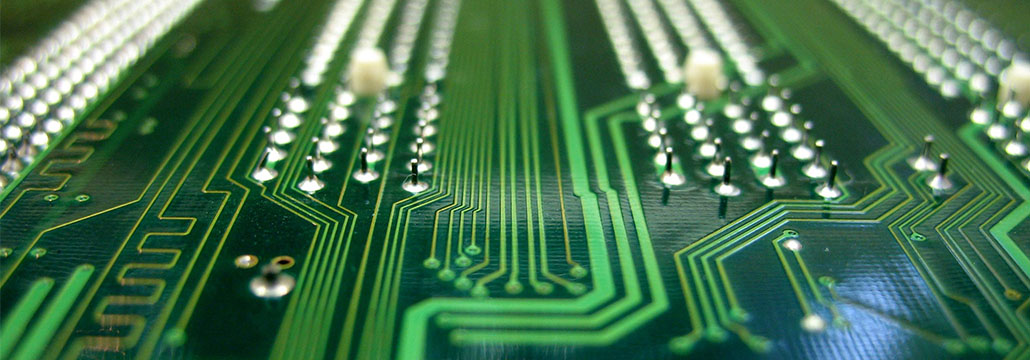
  1. Advanced PCBA Manufacturing and Testing Facilities: Equipped with cutting-edge automated machinery, including advanced printing, surface mounting, and soldering equipment, we ensure efficient production processes and superior product quality.
  2. Premium Quality Materials: We utilize top-notch materials such as high-precision glass fiber cloth and highly conductive copper foil to guarantee excellent performance and reliability of our PCBs.
  3. Advanced Production Techniques: Our expertise lies in utilizing advanced production techniques such as multi-layer boards, high-density interconnect (HDI), and blind/buried vias to meet the demands of complex circuitry while enhancing functionality and reliability.
  4. Rigorous Quality Management System: We have implemented a comprehensive quality management system that covers every aspect from material procurement to production processes. This ensures that our products meet customer requirements and comply with international standards.
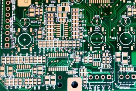
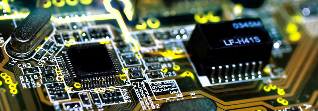
  5. Strong Supply Capability: Equipped with  12 SMT lines, each line has AOI and QC, and each project has an engineer checking who will ensure a 99.7% workable rate for mass production.

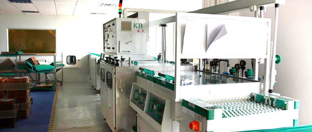
In addition to our state-of-the-art manufacturing capabilities, we have invested in a range of high-end production testing equipment to ensure the quality and reliability of our PCBA products. These include:

Automated Optical Inspection (AOI) Systems:

Utilized to detect defects such as solder joint shorts, open solder connections, and missing components during the assembly process.

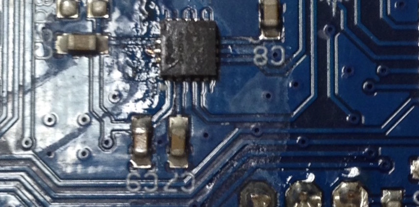
X-ray Inspection Equipment:

Used to inspect internal solder joints and identify defects like cold solder joints, voids, and poor solder connections, providing comprehensive inspection results.

In-Circuit Testing (ICT) Systems:

Employed to test the correctness and performance of electronic components, including resistance, capacitance, and inductance, to ensure compliance with design specifications.

High-Speed Flying Probe Testing Equipment:

Used to test connectivity, signal transmission rates, and other parameters on the PCB, guaranteeing adherence to design requirements.

At our PCBA company, we strive to deliver high-quality products that meet the diverse needs of our customers. With our advanced manufacturing facilities, stringent quality control measures, and cutting-edge testing equipment, we are confident in our ability to provide reliable and innovative solutions for your PCB assembly requirements.

In 2022, China PCB Assembler was the dominating supplier of printed circuit assemblies to the US, making up 58% of US imports.


ENIG PCB (electroless nickel/immersion gold)

Advance in PCB surface preparation

Recently Europe and  US (except for some mil spec and medical applications) resulted in development of lead-free (SAC) solders that are tin-based, with additions of silver and copper and with traces of bismuth, indium, zinc or antimony. Initially, the higher soldering liquidus temperature led engineers to specify high glass transition composite substrates (170°-180°C Tg) but careful attention to reflow profiles allowed a return to the less-expensive standard Tg 135°C FR-4 materials. Since the global industry has moved further toward RoHS, many circuit board manufacturing plants have standardized on Pb-free HAL and no longer price that surface at a premium. Indeed, some have scrapped HASL entirely and subcontract that finish, resulting in a cost premium for leaded solder.

Another option, albeit more expensive than Pb-free HAL, is ENIG (electroless nickel/immersion gold). This surface, like OSP, renders the pads very flat and offers the additional advantage of longer shelf life and the ability to wire bond. There is a low but measurable incidence of gold-to-nickel adhesion failure. This is called “black nickel” or “black pad” (see photo, below right) because, not surprisingly, the surface of the nickel turns black. The immersion gold on the pad surface looks normal and solder wets to the gold quite easily. However, with stress or even vibration the components could easily pop off without warning, the result of a brittle fracture at the interface. There are theories about phosphorous levels in the nickel plating solutions being off-spec and causing intermetallics during the gold plating. This problem is rare but does occur.

The most recent advance in surface preparation is ENEPIG, or electroless nickel/electroless.

How To Present Your Bill Of Materials For Quote

What’s a BOM?
A BOM (bill of materials) is the list of materials and parts needed to produce a product. Clients provide us with a BOM so that we can build their product for them. A BOM inquiry lets us present you with a product quote.
Here at PCB Train we have developed software tools which assist with pricing up your BOM efficiently and accurately. If you follow the 3 tips below your BOM will be priced and sourced using the data you have supplied, without manual intervention from us. This improves accuracy, and speeds up processing. We can happily say that 63% of the BOMs we receive already follow these rules. However, we’re looking to increase this percentage, thus reducing the amount of manual processing needed for those BOMs that need some tweaking.

Facts About PCBs (That You Probably Didn’t Know!)

Why they’re green
Have you ever wondered why the majority of PCBs are that iconic dark green colour? The green that you see is actually the colour of the soldermask showing through the glass. In regards to the origins of the use of the green, there are a few theories.

Some speculate that green was the regulation standard when for when PCBs were used by the American military, and the use of it spread from there. It has also been suggested that green could have been the colour of the original solder mask resins, and that we continue to use green as a matter of convention, despite no longer using these materials. In modern circuits a soldermask can actually be made in any colour. However, green has worked well for us so far, and it makes it particularly easy for engineers to see faults in the traces, so many companies tend to stick with it.

Sitemap | ©Copyright 2023 H.K C-Alley Co., LTD. | Alibaba | KingshengPCBA | All Rights Reserved