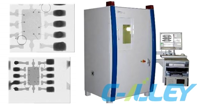
X-Ray for BGA Testing
Automated X-ray inspection (AXI) is a technology based on the same principles as automated optical inspection (AOI). It uses X-rays as its source, instead of visible light, to automatically inspect features, which are typically hidden from view.
As BGA connections are not visible the only alternative is to use a low level X-ray inspection. AXI is able to find faults such as opens, shorts, insufficient solder, excessive solder, missing electrical parts, and mis-aligned components. Defects are detected and repaired within short debug time.
AXI in C-Alley commitments to offering you the complete test and inspection solution.
X-ray inspection is an essential tool in various industries, including electronics manufacturing. It allows for non-destructive testing of electronic components and PCB assemblies to detect faults, defects, or inconsistencies that may not be visible to the naked eye. Here are some specific applications of X-ray inspection in IC, BGA, PCB/PCBA, SMT inspection, and more:
- IC’s Footprint Inspection: X-ray inspection can be used to verify the integrity of IC footprints on the PCB, checking for issues such as peeling, cracking, empty spaces, or wire bonding problems.
- PCB Fabrication Inspection: X-ray scanning helps in identifying welding line offset bridging or open circuits in the printed circuit board.
- SMT Weldability Inspection: It enables the examination and measurement of solder joints for possible defects such as voids or insufficient solder.
- Circuit Line Inspection: Xray testing can detect open circuits, short circuits, or faulty connections within the circuitry.
- Integrity Inspection of Solder Balls: X-ray inspection is utilized to examine the solder balls in array packages and chip covering packaging to ensure their integrity.
X-ray inspection technology has evolved significantly, transitioning from 2D to 3D inspection capabilities. While 2D inspection provides clear images of solder joints on single-layer PCBs, it may encounter limitations when inspecting double-layer reflow soldering PCBs due to overlapping images. In contrast, 3D inspection uses lamination technology to focus on all layers of the PCB and project the corresponding image onto a high-speed rotating receiving surface.
The high-speed rotation of the receiving surface makes the focal point of the image clear, eliminating images from other layers. This enables the 3D inspection method to independently image solder joints on both sides of the PCB, including hidden joints like those on BGAs. It also allows for “slicing” inspection of multi-layer solder joints in BGAs, providing a comprehensive view of the top, middle, and bottom solder ball joints.
Furthermore, 3D X-ray inspection can measure through-hole (PTH) solder joints, ensuring the completeness and quality of solder material within the holes. By connecting the SPC statistical control function with assembly equipment, real-time monitoring of assembly quality can be achieved.
In summary, X-ray inspection, especially with the advancements in 3D technology, plays a crucial role in detecting faults, ensuring the quality of solder joints, and improving the overall reliability of ICs, BGAs, PCBs, and other electronic components and assemblies.


