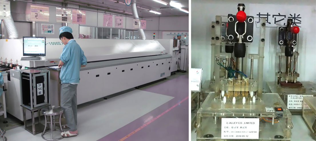
Testing Jig
The testing jig is important so we can spot errors in the PCB before sending it to the final assembly line.
The test jig has two functions:
1) to check that the preamp can hold voltages applied to the power rails and that the supply currents drawn are within tolerance
2) to provide a fast electronic pulse that is applied to the input of the preamp and compare the output waveform to an expected shape. The tester is also designed to be operated conveniently and quickly.
At C-Alley, we do ofen customized test jig design and manufacturing. All the PCBA products must be 100% fully tested.

Testing Jig
To facilitate the fabrication of a test jig, ECAD (Electronic Computer-Aided Design) files are required to automatically identify test points, mounting holes, and other test features. The supported file formats for test jig fabrication include:
- Altium Test Point Reports (.csv)
- Eagle (.brd)
- Gerbers (.zip)
- KiCAD (.kicad_pcb)
When designing the test jig, you can select the appropriate test probe card and receptacle types from a list of compatible parts. You can add, modify, or remove probes and guide pins as needed. Additionally, you can configure the location of the Device Under Test (DUT) and panelization settings to allow for testing an entire panel at once. It is recommended to visually review the generated jig before finalizing the design.
For test jig fabrication, you can download the Design File Package, which includes all the necessary files to build the fixture. These files can be used for fabricating the plates using methods such as acrylic fabrication, CNC milling, or laser cutting.
During the test jig assembly process, you should attach all the probes and guide pins, integrate your test instrumentation, and proceed with running your tests.
In terms of Design for Test (DFT), it is important to consider the following tips to make testing your PCB assemblies easier when using a bed-of-nails style test fixture:
- Place all test points on a single-sided PCB, preferably the side with fewer components. This helps reduce the cost and complexity of the test fixture required for testing the PCB in both rigid and flexible forms.
By following these guidelines and considering DFT principles, you can streamline the test jig fabrication process and enhance the ease of testing your PCB assemblies.

