
• MOB:+86 19879928172
  • E-mail: chinapcba@c-alley.com
C-Alley
  • печатная плата
    • Типы печатных плат
      • Многослойная печатная плата
      • Гибкая печатная плата
      • Жестко-гибкая печатная плата
      • Печатная плата HDI
      • Высокочастотная печатная плата
      • Гибридные ламинаты для печатных плат
      • Печатная плата с металлической подложкой
      • Изготовление печатных плат
      • Прототип печатной платы
      • Быстрый поворот печатной платы
  • PCBA
    • Сборка печатной платы
      • печатные платы
      • Сборка прототипа печатной платы
      • Монтаж поверхностного монтажа
      • BGA-сборка
      • ДИП-сборка
      • Паяльная сборка
      • Сборка коробки
    • Наша сила
      • Производственные возможности
      • Список заводского оборудования PCBA
      • Система контроля качества
      • Комплексный тест
      • Поиск запчастей
      • Гарантия
      • Добавлен сервис
  • EMS
    • Дизайн печатной платы
    • Схематическая диаграмма
    • Компоновка печатной платы
    • Реверс-инжиниринг электроники
    • Расшифровка чипа
    • Копирование и редизайн PCBA
    • Индивидуальная функция
    • Анализ SI-PI-ЭМС
    • Механический дизайн
  • Приложения
  • О нас
    • С-аллея
    • Почему мы
    • оборудование
    • Приходите к нам
  • Новости
  • Связаться с нами
  • Меню Меню

Комплексное тестирование сборки печатных плат

That is an interesting observation about PCB assembly testing procedures. PCBs (Printed Circuit Boards) are indeed a crucial component in most electronic devices, and ensuring their quality and functionality is of paramount importance. PCB assembly testing procedures play a vital role in identifying and rectifying any manufacturing faults or component issues before the end product reaches the consumer.

There are various testing techniques employed during PCB assembly, such as visual inspection, X-Ray for BGA Testing, automated optical inspection (AOI), in-circuit testing (ICT), functional testing, Hi-Pot testing, environmental testing, Burn-in testing, In-process testing, solder paste testing, and burn-in testing.

full range of PCB assembly test services including: 

  • AOI(Автоматический оптический контроль)
  • Функциональное тестирование
  • In-Circuit Testing
  • Испытательный стенд
  • Рентген для тестирования BGA
  • Тест паяльной пасты для печати

Each board is carefully examined by our dedicated inspection team using AOI and high-magnification viewers. Using our X-Ray machine, we test PCBs to the component level and all wiring is fully inspected and tested. Flash testing and earth bonding tests can also be undertaken where required.

Above all, these tests help to detect faults like open circuits, short circuits, incorrect component placement, soldering defects, and component functionality issues. we can improve our production and efficiency through an all-around PCBA test.

Whatsapp Онлайн-чат Пишите нам

Indeed, there are several other PCB assembly tests that can further enhance the quality and reliability of electronic devices. These additional tests focus on specific aspects of the PCB manufacturing process and help identify potential issues or areas for improvement. Let’s explore each of these tests in more detail:

  1. Peel Test:
    This test measures the adhesion strength between the lamination (such as solder mask or protective coating) and the PCB. It ensures that the lamination is securely bonded to the PCB and can withstand stress or environmental conditions.
  2. Solder Float Test:
    This test evaluates the ability of the PCB to withstand thermal stress during the soldering process. It simulates the heating and cooling cycles that the PCB may undergo and ensures that it can handle temperature variations without any damage or warpage.
  3. Solderability Tests:
    These tests determine how well the metal surfaces on the PCB can be wetted by solder. They ensure that the PCB has proper metallization and that solder joints can form reliably. The “Dip and look” method, surface mount simulation test, and wetting balance analysis are common approaches to measure solderability.
  4. Micro-Sectioning Analysis:
    This analysis involves examining the structural characteristics of solder joints under a microscope. It helps identify any defects or anomalies in the soldering process, such as voids, cracks, or improper wetting. Micro-sectioning analysis can be performed on both surface-mount technology (SMT) and through-hole technology (THT) PCBs.
  5. PCB Contamination Testing:
    This test investigates potential contamination on the PCB, including corrosion, degradation, metallization issues, and foreign material presence. Contamination can lead to short circuits or other failures, so identifying and mitigating these issues is crucial for ensuring the reliability of the PCB.

By incorporating these testing procedures into the manufacturing process, manufacturers can fine-tune their manufacturing processes, improve product quality, and minimize the risk of failures or defects. These tests play a significant role in bringing reliable and durable electronic devices to the market.

Оборудование для испытаний сборки печатных плат
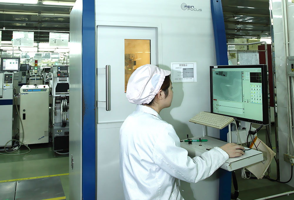
X-Ray

Рентген для тестирования BGA

3D Solder Paste Testing

3D-тестирование паяльной пасты

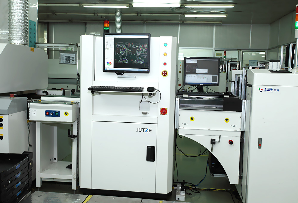
AOI

JUZTE АОИ Тестирование

PCB Testing workshop - PCB Assembly Test

Ремонт BGA

PCBA functional test - PCB Assembly test

Сжечь в тестировании

Point testing - PCB Assembly test

Функциональный тест

  • arrowСборка прототипа печатной платы
  • arrowМонтаж поверхностного монтажа
  • arrowBGA-сборка
  • arrowДИП-сборка
  • arrowПаяльная сборка
  • arrowСборка коробки

Отправить нам запрос

    Последние новости

    • PCBA SMT processing lead timeВремя выполнения обработки PCBA SMT13 октября 2023 г. - 7:59 утра
    • PCBA Applied in Electronic ProductsPCBA применяется в электронных продуктах13 октября 2023 г. - 6:12 утра
    • PCB Assembly approachesТри подхода к обеспечению завершения услуги по сборке печатных плат29 июля 2023 г. - 10:12
    • Меры предосторожности в процессе изготовления прототипа печатной платы25 июля 2023 г. - 8:25
    • 2023 China PCB marketОбзор мирового и китайского рынка печатных плат (pcb), 2023 г.14 июля 2023 г. - 7:21
    • Multilayer PCBs Versus Double-sided PCBsКлюч к высокой производительности: от двусторонних печатных плат к многослойным печатным платам12 июля 2023 г. - 4:14

    О С-аллее

    C-Alley (HK) Co., LTD является специализированным и профессиональнымУниверсальная сервисная компания PCBA и EMSв Китае мы помогаем клиентам с инновациями для услуг по проектированию электроники уже более 13 лет. Мы нацелены на удовлетворение потребностей наших клиентов.

    Адрес: 2/F, корпус 6, 3-я промышленная зона Тантоу, община Тантоу, город Шиян, район Баоань, Шэньчжэнь, Китай, 518108
    E-Mail: chinapcba@c-alley.com
    Тел: 86-755-27202654
    Скайп:Kingsheng.pcba10

    Возможности

    • Дизайн печатной платы
    • Изготовление печатных плат
    • Прототип печатной платы
    • Многослойная жесткая печатная плата
    • Гибкая печатная плата
    • Жестко-гибкая печатная плата
    • Печатная плата HDI
    • Высокочастотная печатная плата
    • Гибридные ламинаты для печатных плат
    • Печатная плата с металлической подложкой
    • Сборка прототипа печатной платы
    • Тест печатной платы

    Сертификаты

    PCB ISO Certificate PCB CE Certificate PCB ROHS Certificate PCB UL Certificate

    Следите за нами

    Мы публикуем новости, касающиеся печатных плат, EMS, печатных плат и нашего корпуса, а также общие новости о нашей отрасли.
    Пожалуйста, посмотрите и следуйте за нами!

    facebook
    twitter
    linkedin
    pinterest
    skype
    Карта сайта| ©Авторское право2026 HK C-Alley Co., LTD.|Алибаба|KingshengPCBA| Все права защищены
    • chinapcba@c-alley.com
    • Kingsheng.pcba10
    • +86 19879928172
    • Онлайн-чат
    • +86 755 27202654
    Пролистать наверх
    • English
    • French
    • Russian