In today’s rapidly developing world of electronic technology, people’s demand for various intelligent devices is growing day by day. One of the core technologies behind these devices is PCBA (Printed Circuit Board Assembly) circuit board assembly technology.As an important component of electronic products, the basic knowledge of PCBA is not only crucial for electronic engineers, but also one of the windows for consumers to understand electronic products. Next, let’s learn about the basic knowledge of PCBA and its important role in the electronic world.
The Basic Concept and Composition of PCBA
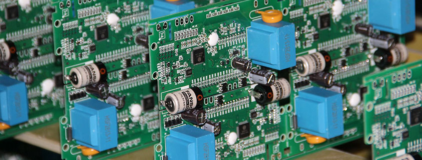
PCBA refers to the process of soldering electronic components (such as capacitors, resistors, chips, etc.) onto printed circuit boards to form a complete circuit board system. PCBA contains multiple important components, the most core of which is the Printed Circuit Board (PCB).
PCB is a board like substrate made of insulating material, on which circuit patterns such as wires and component installation positions are formed through special processes. The design and production of PCBs are the foundation of PCBA, and reasonable layout and precise production determine the performance and reliability of PCBA.
The manufacturing process of PCBA
The manufacturing process of PCBA can be divided into several main steps: preliminary preparation, PCB manufacturing, component installation and welding, testing, and quality control.
Preliminary preparation includes designing schematic and exterior diagrams of circuit boards, selecting materials, etc.
During the PCB manufacturing process, printing, photolithography, electroplating, etching, and other processes are required to ultimately produce pre designed circuit patterns.
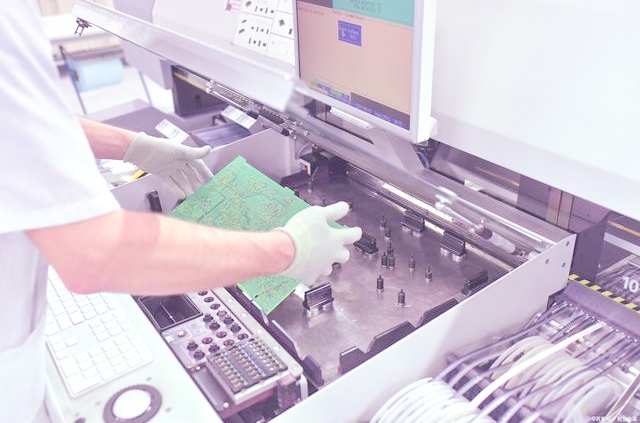
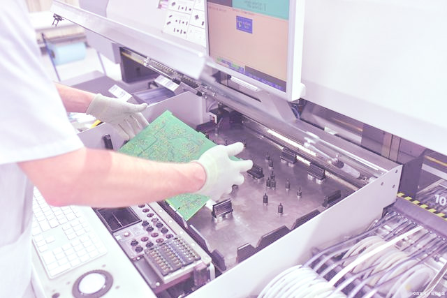
Component installation and welding are crucial steps in PCBA, and precise welding is required based on the component installation position and pins on the PCB.
Finally, through testing and quality control, ensure that the performance and reliability of PCBA meet the requirements.
Development Trends and Challenges of PCBA
With the continuous progress of technology, PCBA is also constantly developing and innovating. On the one hand, with the continuous improvement of electronic product functions, the requirements for PCBA are also increasing, such as higher density and faster speed.
On the other hand, environmental protection and energy conservation also pose new challenges to the manufacturing of PCBA, requiring the use of more environmentally friendly materials and processes.
At the same time, the manufacturing process of PCBA also faces considerations of cost and efficiency. Therefore, the PCBA industry needs to constantly update technology and equipment to meet new challenges.
By understanding the basic knowledge of PCBA, we can better understand the core technologies and manufacturing processes behind electronic products. As an indispensable part of the electronic world, PCBA holds significant importance for both electronic engineers and consumers.
With the advancement of technology, PCBA will continue to develop and innovate, providing more possibilities for the development of electronic products.
China Printed circuit board basic introduction: The PCB application field of the printed circuit board is very wide, covering communication electronics, consumer electronics, automotive electronics, industrial control, medical equipment and aerospace and other electronic information industry major fields. Printed circuit boards have a variety of different classification methods according to the number of conductive graphic layers, substrate type, substrate structure, downstream industry, or technical process standards.
According to the number of circuit board layers: printed circuit boards can usually be divided into single-sided, double-sided and multi-layer PCB board, its main product characteristics and application areas are as follows:
Product Type
Product Features
Main application areas
Single-sided PCB Board
One side of the insulating substrate is covered with copper, and the wire layer and welding pad are made by image transfer method on the copper layer, which is characterized by fast graphic production process, short production cycle, low production cost and high product quality and stability.
Ordinary household appliances, industrial power supply, fast charging sources, car lights and other simple electronic products.
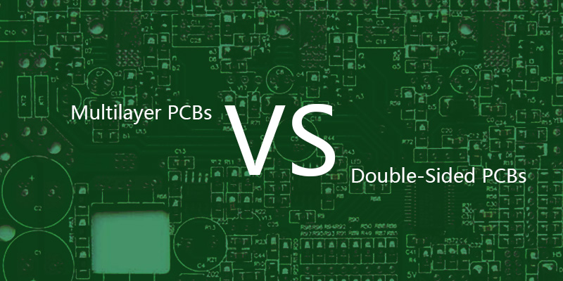
Double-sided PCB Board
A circuit board of circuit structure is arranged on two sides of the insulating substrate, and the two sides of the circuit are connected through a through hole. Compared with the single panel, the application of the double panel is basically the same as the single panel, the main feature is to increase the wiring density per unit area, its structure is more complex than the single panel, and the production process is increased.
Consumer electronics, automotive electronics, communication equipment, industrial control and other fields.
Multilayer PCB board
The biggest difference between PCB multi-layer board and single panel and double panel is to increase the internal power layer and ground layer, with one double-sided inner layer, two single-sided outer layers or multiple double-sided inner layers, two single-sided outer printed circuit board. Through the positioning system and insulation materials are alternately superimposed together and the conductive graphics are interconnected according to the design requirements of the printed circuit board becomes a four-layer, six-layer and more printed circuit board, also known as multi-layer printed circuit board. The power and ground network is mainly routed on the power layer. Multi-layer board wiring is mainly based on the top and bottom layers, supplemented by the middle wiring layer. The design method of a multi-layer board is basically the same as that of double layers, and the key lies in how to optimize the wiring of the internal electrical layer so that the wiring of the circuit board is more reasonable and the electromagnetic compatibility is better. The more layers of multi-layer board, the higher the technical level, and the stronger the technical support ability for the product.
Consumer electronics, battery management systems, servers, automotive electronics, energy storage, 5G communications, medical devices and other fields.
According to the board material division: printed circuit board is divided into the rigid board, flexible board (flexible board), rigid and flexible combined board (rigid and flexible combined board) and other categories, its main product characteristics and application areas are as follows:
PCB Type
Product Features
Main application areas
Rigid PCB board
A printed circuit board made of a rigid substrate that is not easy to bend and has a certain degree of strength can provide support for electronic components attached to it.
Consumer electronics, automotive electronics, industrial control, household appliances and communication equipment.
Flexible PCB board
The printed circuit board made of flexible substrate is characterized by free bending, winding and folding, which meets the development trend of miniaturization, thinness and wearability of electronic products.
Smartphones, laptops, tablets and other portable electronic devices.
Rigid-flex PCB board
A printed circuit board contains a flexible zone and a rigid zone, and the rigid circuit board and the rigid circuit board are laminated into a single component: it can provide the support role of a rigid board, but also has the bending characteristics of a flexible board.
Advanced medical electronic equipment, portable cameras and folding computer equipment.
According to a special process, special substrate division: printed circuit board according to a special process, special substrate division is mainly as follows:
PCB Type
Product Features
Main application areas
Ceramic PCB board
Ceramic circuit board refers to the ceramic substrate covered with copper, drilling, etching lines, surface treatment and other processing processes to form a PCB board with the same electrical interconnection as the circuit board, with good electrical performance, it has good thermal conductivity, excellent insulation performance, high-frequency characteristics, high-temperature resistance, corrosion resistance, pressure resistance, inorganic environmental protection and other characteristics.
5G base station, electronic and electrical, transportation rail, aerospace products, automotive radar and other fields.
Embedded capacity/embedded resistance material circuit board
Capacitance/buried resistance material circuit board refers to the capacitor and resistance into the board inside the product, this product is designed to support more functions, higher clock rate and lower voltage, the capacitor and resistance into the board inside the board to save the surface space of the board, reduce the amount of inductance introduced, thereby reducing the impedance of the power system.
Communication equipment, industrial control, automotive electronics, medical instruments, security electronics, consumer electronics, aerospace and other fields.
High-frequency/high-speed material circuit board
High frequency/high-speed material circuit board using very low-grade signal transmission loss materials, with high frequency and high speed as well as integration, miniaturization, lightweight, multi-function and high-reliability characteristics. Generally, for impedance control, multistage back drilling and other structures of one or more high-rise circuit boards, in harsh environmental conditions can show faster signal transmission speed, less signal delay, and lower signal transmission loss.
Aerospace, automotive radar, 5G base stations, antennas and other fields.
Inlaid with copper columns
Embedded copper column board refers to the different shapes of copper columns embedded into the circuit board internal design products, such product design to support the circuit board local better heat dissipation performance and patch performance, the embedded copper column needs to be with the circuit board design slot or round hole has a high tightness combination.
High power supply, high heat dissipation lamps and new energy battery control module and other fields.
Teflon PCB board
Teflon board is a special circuit board made of Teflon material, which has the characteristics of low transmission loss, low transmission delay, and high characteristic impedance precision control.
Communication base stations, automotive assistance systems, aerospace technology, satellite communications, satellite television, military radar and other high-frequency communication fields.
HDI board is short for High-Density Interconnect printed circuit board, also known as microporous board or laminate board. HDI is a kind of printed circuit board technology, which can achieve high-density wiring and is often used to make high-precision circuit boards. The HDI board is generally manufactured by layering method, and the laser drilling technology is used to drill holes through the layering so that the whole printed circuit board forms the interlayer connection with buried and blind holes as the main conduction mode. HDI board to achieve the printed circuit board of high density, fine wire, small aperture and other characteristics.
Substrate refers to the IC carrier board, which is directly used to carry the chip, which can provide electrical connection, protection, support, heat dissipation, assembly and other effects for the chip to achieve multi-pin, reduce the size of the packaged product, improve the electrical performance and heat dissipation, ultra-high density or the purpose of multi-chip modularization. Packaging substrate is an interdisciplinary technology, involving electronics, physics, chemistry and other knowledge.
Semiconductor chip packaging field.
Analysis of the current situation of the global market: Printed circuit boards were invented in the 1930s and were initially mainly used in military products; In the mid-1950s, printed circuit boards became widely commercially available. After more than 80 years of development, the PCB industry has become the largest output value of the global electronic component industry, and the global PCB market size has reached 60 billion US dollars. In 2020, the economy is under pressure due to the impact of the external environment, but the online behavior spawned by 5G infrastructure construction, cloud computing, big data, and artificial intelligence has stimulated the growth of demand for the electronics industry, and the market demand for China printed circuit boards, as the “mother of the electronics industry”, will continue to show a steady growth trend in the next few years, and the industry will continue to expand.
At present, the PCB industry is in the fifth round of the growth cycle, mainly by 5G to bring cloud computing and the Internet of Things and other technological changes, to help the growth of 5G base stations, communication equipment and new energy vehicles. The total China Printed Circuit Board output value in 2023 has reached $80.92 billion.
With the division of labor in the global PCB industrial chain, the proportion of PCB output value in various countries and regions is constantly changing. PCB supply chain in the early days of Europe and the United States as the center, after World War II gradually developed into a situation dominated by Europe, the United States and Japan, in 2000, the three regions accounted for more than 70% of the global PCB production output value; From 2008 to 2020, the proportion of Europe and the United States gradually decreased, and the proportion of Asia gradually increased, among which mainland China increased the fastest. In 2023, the output value of mainland China was 44.15 billion US dollars, accounting for 54.56%, ranking first in the world, and the total output value of Europe, the United States and Japan was 12.556 billion US dollars, accounting for 15.51%.
Analysis of global PCB output value in 2020-2023
Country and region
2020
2023
2026 Predict
2020-2023
Compound annual growth rate
2023-2026
Compound annual growth rate
USA
29.43
32.46
38.80
10.30%
3.63%
Europe
17.27
20.02
23.81
15.92%
3.53%
Japan
57.71
73.08
91.02
26.63%
4.49%
China Mainland
351.24
441.50
546.05
25.70%
4.34%
Korea
68.81
82.67
100.45
20.14%
3.97%
China Taiwan
82.66
101.82
131.93
23.18%
5.32%
other region
45.07
57.65
83.53
27.91%
7.70%
Sub-total
652.19
809.20
1,015.59
24.07%
4.65%
Product structure: Multi-layer board in the global PCB industry output value accounted for the largest, 2008-2023 annual output value accounted for more than 35% of the total output value of the industry in 2023 multi-layer board output value of 31.053 billion US dollars, accounting for 38.37%; Board output value of 31.053 billion US dollars, accounting for 38.37%; The second is the packaging substrate, the output value of packaging substrate in 2023 is 14.410 billion US dollars, accounting for 17.81%; Flexible board, HDI board, single/double panel accounted for 17.37%, 14.60%, and 11.85%, respectively.
With the trend of technological changes such as automobile electrification and intelligence and 5G bringing cloud computing and the Internet of Things, PCB solutions are diversified, and the market demand for high-density, high-layer, high-tech PCB products will become more prominent. From the traditional multi-layer board-based solution to the metal substrate, thick copper substrate, buried capacity/buried resistance material circuit board, high frequency/high-speed material circuit board, HDI and another special process, special substrate PCB solution evolution.
Analysis of China Printed Circuit Board product structure in 2020-2023
Product structure
2020
2023
2026 Predict
2020-2023
Compound annual growth rate
2023-2026 Compound annual growth rate
Single-double
79.11
95.89
107.79
21.21%
2.37%
Multi-layers
247.63
310.53
371.54
25.40%
3.65%
HDI
98.74
118.11
150.12
19.62%
4.91%
Substrate
101.88
144.1
214.35
41.44%
8.27%
Flexible
124.83
140.58
171.79
12.62%
4.09%
Sub-total
652.19
809.20
1015.59
24.07%
4.65%
Application field: According to the statistics of CICC enterprise letter: Among all kinds of PCB applications in China in 2023, communication accounts for 19.92%, ranking first; Computer accounted for 17.97%, ranking second; Consumer electronics accounted for 14.65%, ranking third; Automotive electronics accounted for 10.79%, ranking fourth. It can be seen that in the China PCB downstream application field, communications, computers, consumer electronics and automotive electronics are the four most important downstream areas. Benefiting from the general trend of automobile electrification and intelligence, the amount of bicycle PCB increases, and automotive PCB will show a significant growth trend by 2026, and the compound growth rate of downstream applications in automotive electronics from 2023 to 2026 will be about 7.91%.
Multilayer PCBs are a kind of printed circuit board composed of alternating conductive graphic layers and insulating material laminated. The number of conductance pattern layers is more than three layers, and the electrical interconnection is realized through metallization holes. If double-sided PCBs are used as the inner layer, two single panels as the outer layer, or two double panels as the inner layer, two single panels as the outer layer, and interconnect with conductive graphics, it can be made of four layers, six layers of printed circuit boards, also known as multi-layer circuit boards.
The production process is to blacken the inner plate pattern first, add the semi-cured layer according to the predetermined design for lamination, then add a piece of copper foil on the upper and lower surfaces, send the press to heat and pressure, to obtain the “double-sided copper clad plate” that has been made of the inner plate, and then carry out CNC drilling according to the pre-designed positioning system. After drilling, the hole wall should be dented and contaminated, and then treated according to the process of double-sided printed circuit board manufacturing.
Compared to the two-panel production process, the main difference between multilayer panels is the addition of several unique process steps: inner imaging and blackening, lamination, dimpling and de-drilling contamination. The same processing process, in terms of process parameters, equipment accuracy, and complexity, there are also some differences. For example, the quality requirements of multi-layer plate hole wall are higher, and the quality requirements of double-layer plate hole wall are higher. In addition, the number of layers drilled in each multi-layer board, the speed and feed rate of drilling, and the difference between the double-sided PCB board. The inspection of finished products and semi-finished products is also more stringent and complex than the inspection of double panels.
Multilayer PCB boards are the addition of an inner layer board on the basis of double panels, usually 4 layers, 6 layers, 8 layers, or more layers. The double panel has only two layers of copper foil, one layer for wiring and the other layer for welding components.
Multi-layer panels have a higher wiring density than dual panels because they can be routed at multiple levels, thus reducing wiring crossover and interference. This makes multilayer PCBs suitable for complex circuit designs and high-density electronic devices.
The multiple-layer PCB board has good electromagnetic compatibility and anti-interference ability because the inner layer board can play a shielding and isolation role. The dual panel is relatively weak in this respect because there are only dual layers of copper foil.
Multilayer boards are more complex and costly than double-sided boards. The manufacture of multilayer panels requires more processes and materials, so its manufacturing costs are higher. At the same time, the design and wiring of multi-layer boards are also more complex, requiring higher technical requirements.
Multilayer circuit board has more advantages in signal transmission and power consumption control. Since the multilayer board can transmit signals and distribute power through the inner layer board, the transmission delay and power consumption of the signal can be better controlled.
In general, multilayer PCBs are more suitable for complex circuit design and high-density electronic devices than dual panels, but their manufacturing costs and design difficulties are correspondingly higher.
Due to the increasingly high functional requirements of electronic products, the structure of PCB boards is becoming more and more complex, from single layer to double layer and then to multiple layers, gradually “evolving”.
In 2022, the global printed circuit board (PCB) design software market size of 100 million yuan (RMB), combined with historical trends and development environment and other factors, it is expected that by 2028, the global printed circuit board (PCB) design software market size is expected to reach 100 million yuan. The Printed Circuit Board Layout Software Industry research report also contains statistics and analysis of the global and China PCB layout software market segments, application markets, and regional market sales, sales, and share changes.
Printed circuit board (PCB) design software industry leaders include Siemens, Altium, Zuken, Autodesk, Cadence, Synopsys, ANSYS, Novarm, WestDev, ExpressPCB, EasyEDA, Shanghai Tsingyue, National Instrument, etc. In terms of revenue, the three major players will hold about 80% market share by 2022.
PCB design software market: Segmentation analysis
In terms of product types, the PCB design software market includes cloud-based, on-premises deployment and other types. In 2022, the market will account for the largest market share, about 70%, and the market size is expected to reach 100 million yuan by 2028. In terms of subdivided application areas, printed circuit board (PCB) design software is mainly used in consumer electronics, computers, telecommunications, industrial/medical, automotive, military/aerospace, and other fields. Among them, the field accounts for the largest proportion, and the market is expected to continue to maintain a leading position in the future.
The global printed circuit board (PCB) design software market is mainly distributed in North America, Europe and Asia Pacific. Among them, the regional market has the greatest potential for development. Germany is expected to maintain its leading position in Europe.
Printed Circuit Board (PCB) design software industry research report with 2023-2029 global and China’s PCB relevant software industry development trend as the research forecast goal, Based on the capacity, product type and application ratio of the Circuit Board design software industry in the past five years, import and export data of major countries, export rankings, key enterprises and other data, analyze and forecast the development prospects and value of the printed circuit board (PCB) design software industry at home and abroad. It is an important basis for enterprises to understand the development direction of the software market and adjust the market layout.
The main contents of the report include the following aspects:
Global and Chinese printed circuit board design software market size, growth rate and revenue statistics and forecasts (historical data 2018-2022, forecast data 2023-2029);
Market Dynamics – Printed Circuit Board design software market overview, development trends, growth drivers, constraints and development opportunities
Market segmentation – Detailed analysis and forecast of market size and growth trend by type, application and region;
Competitive landscape – Analysis of the market performance of major competitors (printed circuit board (PCB) design software market sales, sales revenue, price, gross profit, gross profit margin statistics).
The report is supplemented by a large number of clear and intuitive charts combined with thorough textual analysis to help the industry enterprises accurately grasp the overall scale and development trend of the printed circuit board layout software industry. In addition, the report analyzes and interprets the major enterprises in the printed circuit board (PCB) design software industry, and its product characteristics, market layout, sales model, and development strategy have practical reference value.
Key players in the global printed circuit board (PCB) design software industry include:
Altium
Ansys
Autodesk Eagle
Cadence Allegro
EasyEDA
Shanghai Tsingyue
Zuken
Novarm
Synopsys
ExpressPCB
National Instrument
Breakdown by product type:
Cloud-based computing
Local deployment
Subdivided according to different application areas:
Consumer electronics
computer
telegraphy
Industrial/Medical
CARS
Military/Aerospace
Other
The report focuses on the global printed circuit board (PCB) design software market in North America, Europe, Asia Pacific, and other regions, as well as the main countries in each region, focusing on the analysis of the market position and the overall scale of each region, giving the sales volume, sales and growth rate of design software in the main region, and SWOT analysis of each region. It is conducive for industrial enterprises to accurately grasp the market environment around them.
PCB boards, also known as printed circuit boards, are the carriers of electronic components and an essential element of circuits. They consist of substrates, conductive layers, printing layers, drilled holes, solder pads, and so on. The number of layers in a PCB board is an important factor that manufacturers and designers need to consider in the design and production process. In modern electronic products, multilayer PCBs are widely used.
How many layers can a PCB board have?
Firstly, it is important to understand that the number of layers in a PCB board refers to the number of conductive layers in the board, excluding non-conductive layers such as mechanical support, signal layers, and power layers. Commonly available PCB board layers include single-layer, double-layer, four-layer, six-layer, eight-layer, ten-layer, twelve-layer, etc. Generally, the more layers a PCB board has, the greater the manufacturing difficulty and cost. Therefore, the selection of a PCB board should be based on actual needs.
However, for special applications that require higher layer counts, such as integrating more electronic components on the same board or requiring higher signal transmission speed and lower signal interference, a multi-layer PCB board can be chosen. It is known that the highest number of layers for PCB boards available in the market can reach 60 layers or even more. However, manufacturing such PCB boards is highly challenging and costly, and they are typically used for special high-end applications.
In conclusion, the number of layers in a PCB board is determined by actual needs. In most cases, selecting a four-layer or six-layer PCB board is sufficient for the majority of applications. If a higher number of layers is required, factors such as manufacturing difficulty and cost need to be considered. Therefore, when choosing a PCB board, it is important to consider various factors and select the one that best suits the application’s needs.
On a theoretical level, multi-layer PCB boards can have any number of layers as long as the manufacturing equipment is capable. However, in practice, the most common PCB boards range from 4 to 10 layers, with special military or specific-purpose PCBs reaching over 100 layers. Nevertheless, these multilayer PCBs are not suitable for mass production.
Multilayer PCBs History
In 1961, Hazeltine Corp. from the United States introduced Multiplanar, which was the pioneer in multi-layer board development. This method is similar to the current manufacturing process of multi-layer boards using plated through holes. Since Japan entered this field in 1963, various conceptual designs and manufacturing methods for multi-layer boards have gradually become popular worldwide. As the transition from transistors to integrated circuits occurred and computer applications became more widespread, the demand for high functionality led to the focus on high wiring capacity and transmission characteristics in multi-layer boards.
Initially, three manufacturing methods for multi-layer boards, namely the gap method, the lamination method, and the plated through hole (PTH) method were introduced. The gap method was not practical due to its time-consuming manufacturing process and limited high-density capabilities. The lamination method, although offering high density, was complex and not as urgently needed at that time. However, as the demand for high-density circuit boards grew, the lamination method became a focal point for research and development by various manufacturers. Currently, the PTH method, which shares the same process as double-sided boards, remains the mainstream manufacturing method for multi-layer boards.
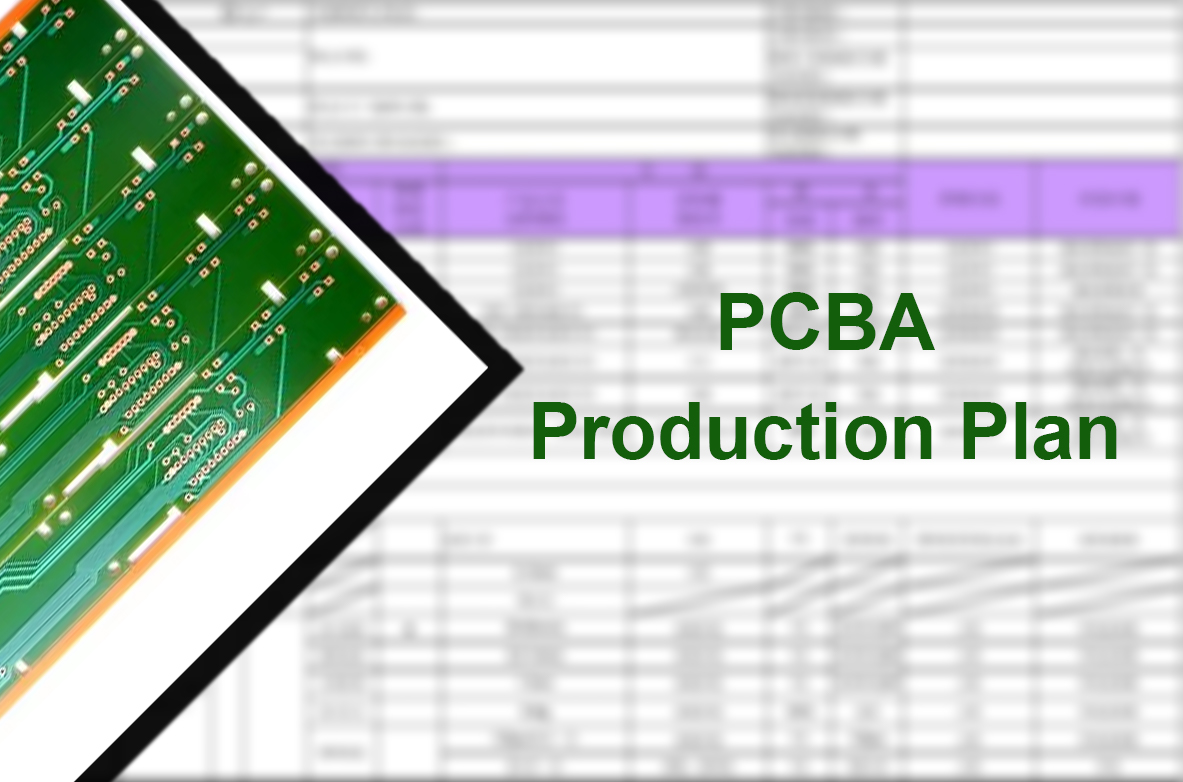
PCBA Order Management System(OMS): Through the order center, the management of orders, including order receipt, order confirmation, payment receipt confirmation, automatic matching warehouse, inventory control, automatic matching express delivery, and a series of collaborative operations in the order life cycle. The relevant process is as follows:
Receive PCBA order after quote
Confirm the customer order content: the order contains a series of order data such as the order name of the customer and the name of the person under the order, the order name of the manufacturer and the contact person, the product name, the quantity, the unit price, the total amount, and the shipping address.
Confirm whether the customer’s payment has been received: After the financial department confirms that the payment has been received, it will be entered into the ERP system, and the order will be sent to the factory to inform internal production.
Make production plan
All departments shall reply with the required materials within 2 hours of receiving the production notice;
PMC determines the order delivery time according to the production capacity and raw material purchase cycle, and informs the merchandiser of the internal evaluation delivery time;
Material preparation production
The purchasing department shall purchase materials according to the material type, specification, manufacturer, and packing method specified by the customer according to the production plan after receiving the material quota. After the materials are assembled, the factory will arrange the production according to the SOP process on the work order issued by the project.
Follow-up order production
The merchandiser needs to keep in close contact with the factory, keep abreast of the production situation at any time, and timely feedback to the customer when the delivery is abnormal.
Warehousing of goods
Confirm the delivery time and method with the customer after the goods are produced and stored.
Inspect Goods
In order to ensure that there is no problem with the quality of the final PCBA products, OQC needs to inspect the goods before delivery, and the business needs to confirm the bar code on the label of the outer box and the special identification requirements of the customer.
The service provides a Packing List (including the number of goods, box size, weight, number of pieces, specifications, etc.) to freight forwarders or express pickers.
Arrange Delivery
If it is EX works terms, 1-2 days in advance with the customer to confirm the express method or customer freight forwarder to pick up the goods.
If the terms are FOB, book the space with the freight forwarder 2 weeks in advance and get the SO (Shipping Order), the PCB Assembly factory’s delivery time and shipping date will be connected on time to meet the delivery date specified by the customer.
If the seller pays the freight (CIF, CNF), consult the shipping company or shipping company 1 week in advance about the shipping date, freight rate, port of departure, etc. After comparison, choose the shipping company with a favorable price, good reputation, and suitable shipping schedule, and inform the customer to confirm.
Customs Declaration
After loading the container, the documents required for customs clearance will be handed over to the cooperative customs broker, and the export customs clearance will be entrusted.
Usually, two days are allowed for customs clearance (before the ship closes). Consignment customs declaration should provide loading information, including the loaded goods and quantity, port, shipping company, warehouse number, container number, ship opening and closing time, trailer company, container type, and quantity, the company’s contact and telephone number, etc. (these are generally freight forwarder and customs broker contact arrangements).
The professional customs declarant shall go through the customs clearance formalities with the packing list, commercial invoice, declaration letter, export settlement, verification form, copy of export goods contract, export commodity inspection certificate, etc.
Customs clearance procedures for import and export goods include acceptance of declarations, examination of documents, inspection of goods, taxation, customs clearance, and release.
24 hours before loading, declare to customs (i.e., declare to customs) and submit various documents: Export goods declaration form: The customs declaration form is the basic document for the customs to supervise, inspect, collect taxes, and make statistics on the export goods. Export license: A unit with the right to export shall export commodities that are not subject to license administration within its business scope. If the export exceeds its business scope, and the State stipulates that an export license must be applied for, the export license or other approval documents stipulated by the State shall be submitted to the Customs for examination. Shipping Order or shipping order: A shipping note is a document issued by a shipping company to the shipper informing the ship of shipment. After the customs inspection and release, the loading bill or waybill shall be stamped with the release seal and sent back to the customs declaration for shipment of the goods for export. Commercial Invoice: Invoice is an important basis for customs to collect duties. Packing List: It is a detailed supplement to the contents of the invoice. Export receipt verification: The documents provided by the foreign exchange control department shall be stamped by the customs after completing the customs clearance procedures, and the foreign trade company shall settle the foreign exchange with the foreign exchange control department for verification and cancellation. Trade contracts: Certificates of origin and other relevant certificates which the Customs shall submit for inspection when it deems necessary.
Submit Shipping Documents To the Customer
Deliver shipping documents: packing list, invoice, OQC report, customs declaration, etc. to the customer on the day of shipment and inform the customer of the estimated time of arrival at the destination.
After-sales service
For example, if a customer complains about an order, whether it is damage to the outer box during transportation or poor product function found during client production, the sales team needs to effectively handle the hospitality complaint with the internal team in the fastest time.
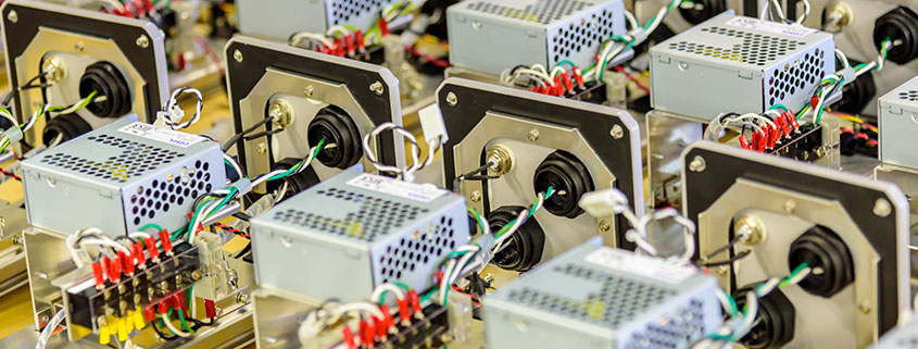
In the highly competitive world of electronics manufacturing, efficiency and reliability are critical to success. One key component of this process is box build assembly. It refers to the process of assembling all of the internal components of an electronic device into a finished product, ready for use by the end user.
The importance of box build assembly cannot be understated. Proper assembly ensures that the final product is both efficient and reliable. A poorly assembled device may function erratically, leading to customer dissatisfaction, increased warranty costs, and possible brand damage.
To address these challenges, many electronics manufacturers turn to complete box build assembly solutions. These solutions provide a comprehensive approach to the assembly process, ensuring a smooth and efficient process from start to finish.
The solutions offer a range of benefits, such as increased control over the manufacturing process, enhanced quality control, streamlined supply chain management, and reduced time to market. These benefits translate into increased competitiveness and improved bottom line performance.
Choosing the Right Provider
But not all complete assembly solutions are created equal. It is important to partner with a provider that offers a range of services to meet your specific needs. This may include design support, prototyping, testing, customization, and logistics support.
In addition to these services, it is also important to consider the level of experience and expertise of the provider. Choose a provider that offers a proven track record of success, and a team that is knowledgeable about the latest technologies and best practices in the industry.
In conclusion, complete solutions are a critical component of efficient and reliable electronics manufacturing. By partnering with an experienced provider that offers a range of comprehensive services, manufacturers can streamline their operations, reduce costs, and improve their competitiveness in the marketplace.
In today’s world, electronic devices and circuits have become an integral part of daily life. The gadgets we use daily like phones, computers, television, and cars have all become smarter and more complex, thanks to the advancement of PCB assembly technology. PCB, or Printed Circuit Board, is a critical component of these electronic devices that connect all the electronic components, ensuring their proper functioning. The high-precision PCB assembly service not only offers a seamless solution to the electronic industry but also helps to improve the reliability, accuracy, and durability of electronic devices.
With the rise of a diverse range of electronic devices, select PCB assembly providers have specialized in offering one-stop electronic component services to their customers. This service offers a comprehensive solution to the manufacture of complex electronic devices, including the customer’s product idea to the finished product. These one-stop services include prototyping, design, fabrication of the printed circuit board, component procurement, surface mount technology (SMT), manual through-hole assembly technique, functional testing, and final assembly. This approach is convenient for their customers because it eliminates the need to interact with multiple service providers, resulting in product quality control from start to finish while saving time and costs.
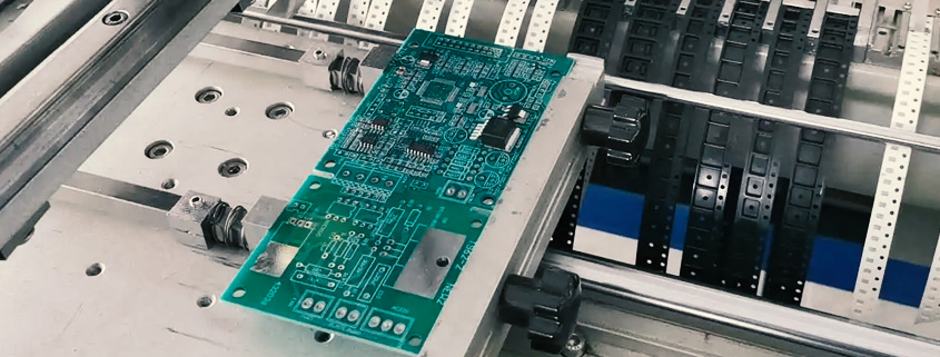
High-precision PCB assembly often entails the latest PCB assembly technologies, including surface-mount technology (SMT), which involves the attachment of electronic components on the surface of PCBs. This technique has several benefits. First, it enhances the circuit board’s reliability by reducing the connection wires. Second, SMT enables the PCB to have more components assembled into it, increasing the functionality and performance of the device. Third, SMT consumes less space, making it suitable for the fabrication of smaller PCBs.
On the other hand, the manual through-hole assembly technique helps to connect electronic components on the opposite side of the PCB surface. This technique is suitable for electronic devices requiring a stable mechanical and chemical bond between the components and the PCB, compared to the less stable solder joints obtained from SMT.
The one-stop PCB assembly service providers pride themselves on their quality control measures to ensure that all components and PCBs assembled conform to the customer’s specifications. They have quality control procedures that ensure that individual components meet set standards, the assembly process flows systematically according to a set procedure, and inspection methods are undertaken after assembly to verify the integrity of the electronic devices in the final assembly stage.
In conclusion, the high-precision PCB assembly service provides a one-stop electronic component service that offers a comprehensive solution to customers’ electronic component fabrication needs. These services not only provide quality assurance to electronic devices but also save time and costs incurred through interacting with multiple service providers. PCB assembly and its relevant technologies continue to evolve, and it’s essential for service providers to keep up-to-date with the changing trends. This will give them a competitive edge in the market while offering superior service to their clients.
As a buyer of printed circuit board Assembly(PCBA), it’s normal to focus on the price and quality of the components when making your purchase decision. However, have you considered the importance of post-purchase support?
PCBA after-sales support refers to the services and guidance provided after the purchase of a PCBA. It is a vital component of the overall purchasing experience, as it helps you make the most of your investment and avoid potential issues that can lead to downtime, production delays, and higher costs. In this article, we’ll explore the benefits of strong after-sales support and why it’s critical to customer satisfaction.
Supporting Your Business with PCBA After-sales Support
Expert Technical Assistance:
The primary advantage of strong PCBA after-sales service is expert technical assistance. Suppliers who offer top-quality support have experienced engineers to help you troubleshoot problems with the assembly, set-up, and operations. Technical assistance can range from online manuals, data sheets, and tutorials to on-call support and on-site visits. These experts can help you optimize the PCBA’s performance, avoid downtime, and reduce the risk of quality issues.
Warranty and Repair Services:
C-Alley provides a free replacement within 3 years if major problems caused by us and free of charge repairing for sold PCBAs within 5 years. Robust after-sales support also offers warranties and repair services for their products. Providers stand by the quality of their products, and they offer a warranty to protect customers against defects or damages that may occur after delivery. In case of issues, repair services are available to restore the PCBA to its proper working condition. These warranties and repair services help you save money and avoid inconvenience and delays in your production schedule.
Customization and Upgrades:
Strong PCBA after-sales support also provides customization and upgrade services. These services include functionality upgrades, component substitutions, customization of the PCBA layout, and firmware or software upgrades. Customization and upgrades ensure that the PCBA meets your specific needs and requirements, enhances the PCBA’s functionality, and extends its useful life to maximize your ROI.
Feedback and Continuous Improvement:
The best PCBA after-sales support also provides feedback channels and continuous improvement programs. Feedback channels allow customers to share their experiences, issues, and feedback with the support team, which can be used to improve product quality, support services, and processes. Continuous improvement programs help suppliers increase production quality, reliability, efficiency, and cost-effectiveness. As a customer, you benefit from these programs, as they ensure that your products are up-to-date, innovative, and efficient.
In conclusion, PCBA after-sales support is a critical factor for maximizing your ROI and achieving post-purchase satisfaction. Strong PCBA after-sales support includes expert technical assistance, warranties and repair services, customization and upgrades, feedback channels, and continuous improvement programs. When selecting your PCBA supplier, make sure to prioritize one that offers robust after-sales support services. This way, you can rest easy, knowing you will get the support and services necessary to ensure an optimal post-purchase experience.
If you manufacture printed circuit boards (PCBs), one of your main concerns should be quality control.It encompasses all the processes and procedures put in place to ensure the reliability, durability, and proper functioning of the PCB board. In this guide, we’ll take a look at the importance of quality control for PCB boards, as well as tips for ensuring quality control during the board manufacturing process.
The Importance of PCB Board Quality Control
Quality control ensures that the board meets the required standards for functionality, reliability, and durability. Poor-quality PCB boards can lead to product malfunctions, customer complaints, and costly product recalls. PCB defects can also result in downtime, loss of productivity, and decreased production efficiency.
Tips for Ensuring Quality Control during PCB Manufacturing
Proper Design and Manufacturing: To ensure quality control, the PCB board must be designed and manufactured correctly. Consider partnering with PCB board manufacturers who have a proven track record of producing high-quality PCB boards. Ensure that the manufacturer follows a detailed and standardized production process, from design to testing and delivery.
Rigorous Inspection and Testing: Inspection and testing are critical steps in ensuring the quality of the PCB board. During production, each PCB board should undergo strict inspection by qualified technicians to ensure that all parts are correctly placed and soldered. Additionally, each finished PCB board should be subjected to rigorous testing to confirm that it meets the required standards of functionality and reliability.
Compliance with Industry Standards: Keep in mind the industry standards and regulations regarding PCB board manufacturing. Ensure that your PCB board manufacturer complies with these standards to ensure that the PCB board meets the required quality levels. Non-compliance with industry standards and regulations can lead to product recalls and even legal liabilities.
Documented Processes: To ensure quality control in the PCB board manufacturing process, it’s essential to have clear and well-documented procedures that outline production processes, testing and verification methods, and quality standards. This way, you can ensure that your manufacturer follows the right processes, resulting in high-quality PCB boards that meet industry standards.
Conclusion
In conclusion, quality control in the manufacturing of PCB boards is essential for ensuring product reliability and durability. To ensure quality control, it’s crucial to select a reliable and experienced PCB board manufacturer that follows strict production processes, rigorous testing and inspection protocols and complies with industry standards and regulations. With these tips, you can manufacture quality PCB boards that meet the highest standards of reliability and functionality.