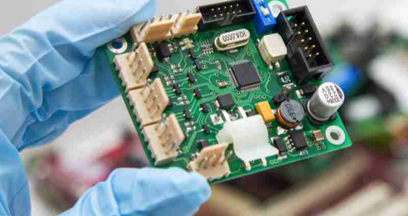
Why SMT

Why SMT?

Surface-mount technology (SMT) is a method for producing electronic circuits in which the components are mounted or placed directly onto the surface of printed circuit boards (PCBs). An electronic device so made is called a surface-mount device (SMD).

An SMT component is usually smaller than its through-hole counterpart because it has either smaller leads or no leads at all. It may have short pins or leads of various styles, flat contacts, a matrix of solder balls (BGAs), or terminations on the body of the component.

Why SMT?

Mass produced electronic circuit boards need to be manufactured in a highly mechanised manner to ensure the lowest cost of manufacture. It need passive SMDs (Resistors and capacitors),Transistors and diodes, Integrated circuits should be packaged in reels / Reels.

PCB Production Steps

PCB production Steps

PCB Etching Process

All PCB’s are made by bonding a layer of copper over the entire substrate, sometimes on both sides. Etching process has to be done to remove unnecessary copper after applying a temporary mask, leaving only the desired copper traces.

Though there are many methods available for etching, the most common method used by electronics hobbyists is etching using ferric chloride ir hydrochloric acid. Both are abundant and cheap. Dip the PCB inside the solution and keep it moving inside. Take it out at times and stop the process as soon as the copper layer has gone. After etching, rub the PCB with a little acetone to remove the black colour, thus giving the PCB a shining attractive look. The PCB layout is now complete.

PCB Drilling

The components that have to be attached to the multi-layered PCB can be done only by VIAS drilling. That is, a pated-through hole is drilled in the shape of annular rings. Small drill bits that are made out of tungsten carbide is used for the drilling. A dremel drill press is normally used to punch the holes. Usually, a 0.035 inch drill bit is used. For high volume production automated drilling machines are used.

Sometimes, very small holes may have to be drilled, and mechanical methods may permanently damage the PCB. In such cases, laser drilled VIAS may be used to produce an interior surface finish inside the holes.

Conductor Plating

The outer layer of the PCB contains copper connections (the part where the components are placed) which do not allow solderability of the components. To make it solderable, the surface of the material has to be plated with gold, tin, or nickel.

Solder Resist

The other areas which are not to be solderable are covered with a solder resist material. It is basically a polymer coating that prevents the solder from bringing traces and possibly creating shortcuts to nearby component leads.

PCB Testing

In industrial applications, PCB’s are tested by different methods such as Bed of Nails Test, Rigid Needle adaptor, CT scanning test, and so on. The basic of all tests include a computer program which will instruct the electrical test unit to apply a small voltage to each contact point, and verify that a certain voltage appears at the appropriate contact points.

Basic process to assembly PCB board with components

Basic process to assembly PCB board with components.

As a China original PCBA manufacturer ,we do PCBA board according to Bom list & Gerber files via SMT machines & DIP assembly.
Below is the basic process to assembly PCB board with components.
1.Confirm the necessary files and order details.
2.Order and receive the SMT paste stencil if necessary.
3.Program our machines from the BOM and Centroid file, before the materials arrive.
4.Materials are received in. Materials are audited before your job is run.
5.If all materials are in before noon, the assembly clock starts that day. If after noon, the clock starts the next day.
6.A SMT stencil and stencil printer are used to mechanically apply the paste.
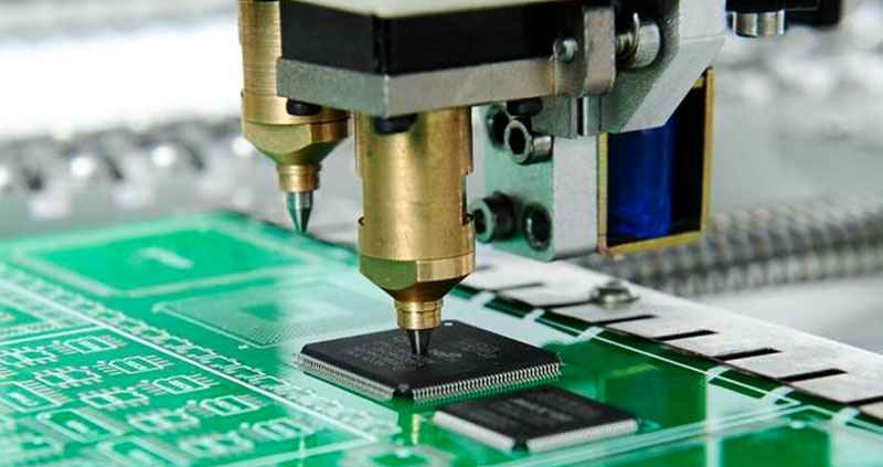
7.An automatic pick and place machine place the SMT components.
8.A SMT reflow oven is used to reflow the solder onto the SMT components.
9.BGA components are X-rayed to verify placement accuracy and to detect any solder bridges.
10.Thru-hole parts are inserted by hand. They may also be wave soldered depending on the board layout.
11.A 100% final quality check is performed.
12.The finished PC board assemblies are shipped back to you.
C-Alley PCB Assembly & Prototyping services

C-Alley PCB Assembly & Prototyping services

C-Alley’s offers PCB prototyping services utilizing dedicated automated pick and place equipment for samples making & mass production for high quanlity PCBA circuit board.
A distinguishing feature of C-Alley’s turnkey manufacturing solutions is our Transparent Pricing. Open BOM to list the cost of each components, you can check our profit point only wthin 5~10%, Transparent Pricing includes a line by line costing of the Bill of Materials, labor costs, profit margins. It’s truly open-book pricing. It allows AMI and its customers to work jointly at reducing costs which make everyone more successful in the end.

As a  PCBA manufacturer ,we ensure 99.7% workable PCBA, but 100% yeild by function testing, but how can we guarantee such high passing rate ? modern high-tech PCBAs can potentially have 20,000–30,000 solder joints, requiring sophisticated automated inspection techniques to efficiently inspect results and provide process control feedback. The solutions is to set up a series testing instructions such as programming and function test.

 In a high-mix environment C-Alley typically deploy automated optical inspection (AOI), automated x-ray inspection(AXI), and flying probe (FP). By endeavoring to minimize test element overlap, we minimize both programming and runtimes.
Our strengths
Surface Mount, Through-Hole, or Mixed Technologies
BGA placement down to 0.2mm pitch
Chip placement down to 0201,01005 packages
Machine-placed prototypes,PCB prototypes
IPC-610 Class III Workmanship with certified in-house trainer
Extensive automated production equipment
X-Ray and Automated Optical Inspection for BGA
Coating and Encapsulation Services
Why the etch pads are not big enough for vias

Why the etch pads are not big enough for vias

Now C-Alley is using the leading edge technologies such as ball-grid arrays (BGAs), chip scale packaging, flip chips, QFNs, DFNs, and others. It shines x-ray radiation through a component package like a BGA to view images including wire bonding, solder joints, and solder defects, if any. Standard x-ray inspection is used for simple applications, whereas high-end x-ray is used to detect such defects as head-on-pillow, disjointed balls on a BGA package, wire bonding damage, and other similar problems.

C-Alley is a PCBA manufacturer who is dedicated to offering high quality PCBA products to worldwide customers. Please send us your Gerbers and BOM,we’ll quote for your A.S.A.P.

Today we’re going to discuss about the problem that why the etch pads are not big enough for vias?

As designs get more compressed, conductors, spaces and pads continue their march to be smaller and smaller. Designers are left trying to squeeze pad sizes in order to route traces within BGAs or other tight component packages.

There is often confusion related to drawing requirements for drilled holes and the sizes manufacturers actually drill to achieve the drawing requirements. Let’s clear that up and talk about strategies to gain as much room as possible, while maintaining adequate annular ring.

First, let’s not forget fillets at the via-to-trace transition. This is absolutely required, especially if Class 2 annular ring is called out. It provides a level of insurance against breakout at the via-to-pad transition, which could lead to an open circuit. It is also good design practice, as it improves etch quality and provides mechanical strain relief, reducing potential for cracking.

So what’s the deal with drilled holes? We will concentrate here on mechanically drilled holes, not laser microvias. (That is a topic for another day.) When a drawing calls out a hole size, it will usually have a tolerance, such as 0.010″+/-0.003″. When this happens, the PCB manufacturer must select a drill size that compensates for all processing so the finished hole will meet the drawing requirement. The manufacturer will aim for the center of the drawing window, so in the case of 0.010″+/-0.003″ they will try to finish at 0.010″ or slightly above that. If the tolerance is not centered on the nominal hole – e.g., 0.010″+0.002″/-0.004″ – they will aim for the middle of the range, in this case 0.009″.

To make this work, they will add allowances for copper plating and final finish to the finished size. Typically, they will drill about 0.002″ to 0.003″ above the maximum allowable finished hole size. In the case of our example, they will drill at 0.015″.

This eats into the annular ring, especially for the internal layers. Say you designed a 10 mil pad and coupled that with a 20 mil pad, and thought you had plenty of room. However, the internal layers are now down to 2.5 mils of annular ring at design. Making IPC minimums for internal annular ring on the finished product will be unlikely.

Sitemap | ©Copyright 2023 H.K C-Alley Co., LTD. | Alibaba | KingshengPCBA | All Rights Reserved