2016 China Printed Circuit Board (PCB) Industry

2016 China Printed Circuit Board (PCB) Industry

The China Printed Circuit Board (PCB) Industry 2016 Market Research Report is a professional and in-depth study on the current state of the Printed Circuit Board (PCB) industry.

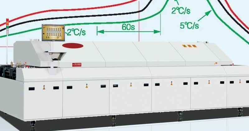
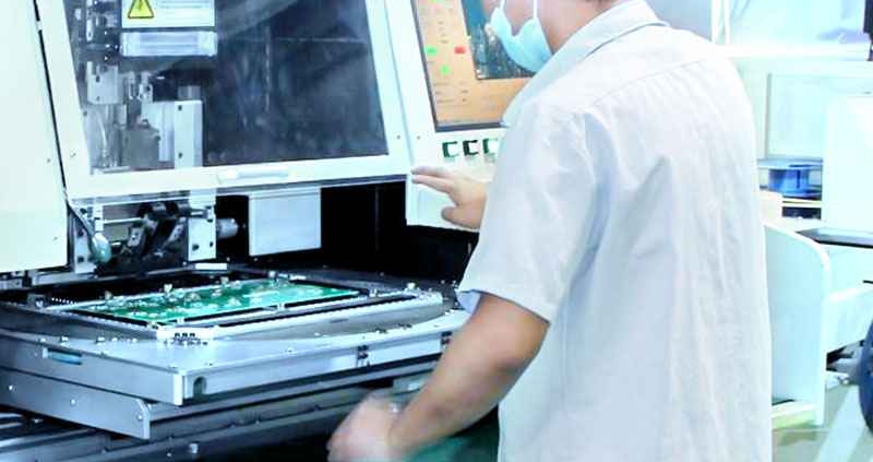
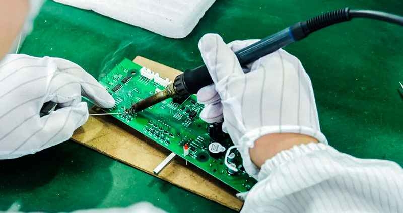
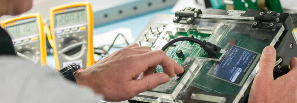
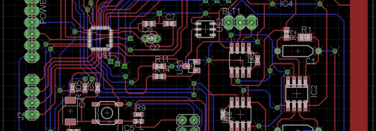
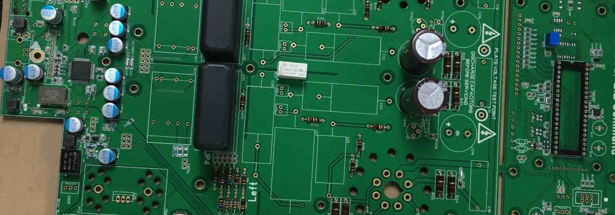
The China Printed Circuit Board Industry provides a basic overview of the industry including definitions, classifications, applications and industry chain structure. The Printed Circuit Board market analysis is provided for the international markets including development trends, competitive landscape analysis, and key regions development status. Development policies and plans are discussed as well as manufacturing processes and cost structures are also analyzed. This report also states import/export consumption, supply and demand Figures, cost, price, revenue and gross margins.

Over the five years through 2016, revenue for the Printed Circuit Board Manufacturing industry has increased at an average annualized rate of 8.1% to $78.9 billion. As printed circuit boards are intermediate components, the majority of industry revenue is derived from sales to downstream wireless industries and consumer electronic manufacturing industries. Growing household income in China has led to increasing demand for electronic products, boosting demand for printed circuit boards.

Growth in the Printed Circuit Board Manufacturing industry in China has gradually slowed in recent years. In 2016 alone, industry revenue is expected to grow 6.5%.

The Printed Circuit Board Manufacturing industry has grown rapidly over the past five years. In 2016, industry revenue is expected to reach $78.9 billion. High growth has been driven by greater domestic and foreign demand.

As printed circuit boards are an intermediate product, the majority of industry revenue is derived from sales to downstream wireless industries and consumer electronic manufacturing industries. Growing household income in China has led to increasing demand for electronic products, creating demand for printed circuit boards. However, wireless and consumer electronics industries are subject to rapid technological change, which brings about intense competition, short product life cycles and significant fluctuations in product.

PCB practical certifications

A PCBA leader with certifications

C-Alley is a Chinese PCBA leader and one of the leading assember of high-value/requrements printed circuit boards . The core business segments are Smart home application Devices, Automotive, Industrial, Medical and Advanced Packaging. In 2016, C-Alley has extened the global presence to Austria, Europe, USA, The Middle East and Russia.  our factory bring an enviable number of quality approvals and certifications including ISO 9001, ISO 1400 and ISO/TS 16949, full UL Recognition.

Now we’ll focus on the production tech of extremely compact substrates/modules, advanced heat management, Embedded Component Packaging , HF printed circuit boards (PCBs) and flexible PCBs for medical devices .

Welcome to send a quote to :  [email protected] , and better to attach Gerber file & Bom list, thank you!

Printed circuit board sales on 2016

Printed circuit board sales on 2016

Taiwan is considered the top-producing country for circuit board production (including manufacturing from China). Monthly shipments of printed circuits from Taiwanese manufacturers increased for both second and third quarters. Most of this increase was from the robust sales of PCs. New products from Apple dramatically increased the sales of flexible circuits until the month of September where shipments posted a negative result comparing month over month. Revenue for the Taiwanese industry lost its momentum during the 4th quarter. Year to date revenue through October was 2.7% less than the same period of time last year. I am not too optimistic sales will increase for the last two months of the year, so my prediction is that annual revenues will decrease by 3% compared to last year. This will be the first negative result since the global recession in 2009.

Revenues for the Japanese printed circuit industry are also disappointing. Year to date through September, revenue declined 10.4% compared to the same period last year. This drop in revenue can be attributed to a 6.3% decrease in shipments. Unfortunately, printed circuit manufacturers have to trim their margins to remain competitive in this limited market. The major market for rigid board manufacturers in Japan come from domestic mobile products that includes smartphones. Unfortunately, market share for Japanese equipment manufacturers has been eroding all year, so I am pessimistic for a rebound during fourth quarter.

Flexible circuit manufacturers are performing the worst. Revenue decreased by 20.1%, and volume declined by 8.9% through September comparing year-over-year. These flex manufacturers might have to lower prices. Their largest customers are smartphone companies from other countries, and pricing is extremely competitive from Taiwanese and Korean flex circuit manufacturers. Year to date revenue from module circuit manufacturers (mostly substrates for semiconductors) increased 0.2% during the first three quarters of this year compared with last year. Unfortunately, revenue declined by 10.2%. The global semiconductor market grew during the same period. Japanese module circuit manufacturers continue to lose market share. Total sales from the Japanese printed circuit industry will decline about 10% in 2016. This will be the largest market decline since the global recession in 2008 and 2009.

The printed circuit industry in North America posted relatively small growth results during the first three quarters in 2016. I was predicting a 4 to 6% growth this year, however, shipments and pre-booked orders slipped by double digits from September to October. This decline is different from normal seasonal fluctuations. YTD revenue for the first 10 months posted a 2.8% growth compared with the same period of time last year. This is a significant pull back from the previous months. Both revenue (-8.3%) and pre-booked sales (-1.8%) for October indicate a negative result comparing month-over-month versus last year. The industry forecast does not show an optimistic outlook for the last two months of the year. Industry growth for the North America market will be about 1% less than the previous year.

Germany is the largest printed circuit producer in Europe. Industry growth for the first eight months of the year is negligible: however, YTD revenue for the first 8 months decreased by 0.1% compared with the same period of time last year. Fortunately, orders increased recently, and the industry is forecasting a positive growth for 2016.

Totally,we may need to think about the action plans before the new year, hope to have a big crop in 2017.

Reflow oven temperature during SMT production assembly

Reflow oven temperature during SMT production assembly

SMT production assembly involves heating the PCB in a reflow oven. Oven temperatures are high, ranging to about 260°C. This heat spreads over the surface of the PCB. In the event thermal imbalance exists, such that during the soldering, substantial temperature differences are generated between two points on the PCB’s surface (ΔT) (more than 7°C), the PCB will experience thermal shock during heating in the oven. The result of this thermal shock may be PCB warpage, insufficient soldering for certain components, and other defects.

This phenomenon is greatly affected by component location on the PCB. Parts on the PCB are heterogeneous and may include small passives (resistors, capacitors, inductors) whose heat signature is low, together with large actives (BGAs, LGAs) whose heat signature is high. The concentration, on one hand, of components whose heat signature is high in a certain area of the PCB, and on the other hand, the concentration of components whose heat signature is low in another area of the PCB, may cause significant temperature differences between those two areas and instigate thermal shock.

Therefore, during PCB design, it is very important to ensure thermal balance is maintained on the PCB. One recommended method to prevent thermal shock is to uniformly distribute components whose soldering temperature is high across the PCB surface, rather than place them all in a certain single area.

Another way to maintain thermal balance is to ensure the PCB layer stack-up is symmetrical, that is, ensuring the copper and ground layers are evenly divided from the center of the PCB toward the top and bottom layers of the board (FIGURE 2).

nistec2
FIGURE 2. PCB layer stack-up design.

high temperature for pb-free assembly

High temperatures of Pb-free assembly

C-Alley is offering the services of global PCB assembly & manufacturing, PCB layout & design , reverse engineering.

Few projects during PCB assembly may have below errors if designer do not pay attention to it.

The PCB production cycle includes two main stages: fabrication of the PCB and assembly of components on the PCB. Variations in these processes are ripe for incompatibilities. This can occur, for instance, when raw materials for fabrication are optimized for SnPb technology, yet the PCB is assembled using Pb-free technology. SnPb technology assembly is characterized by relatively low temperatures: for instance, raw material possessing a 130Tg. (Tg is glass transition temperature, or the temperature at which the raw material traverses from a solid-rigid state to a flexible-elastic state.) Pb-free assembly is characterized by high soldering temperatures, about 40°C higher than that of SnPb assembly. When a PCB whose raw materials are suited to low assembly temperatures is assembled using higher-temperature Pb-free technology, the PCB will warp during reflow. In this case, it would have been appropriate to define for fabrication raw materials with a higher Tg, such as 170, to ensure the PCB withstands the high temperatures of Pb-free assembly.

High temperatures of Pb-free assembly

It’s not ok to place components at the edge of a PCB (< 5mm)

The PCB traverses stations on the assembly line on a conveyor belt. This conveyor belt, which is located along (almost) the entire production line, is composed of two parallel tracks. These tracks comprise a small depression that enables the PCB’s stability on the conveyor belt. The projection of the depression’s area on the PCB is unreachable by the placement machine head. Therefore, no components should be placed in that area. Placing components at the edge of a PCB (< 5mm) may make it difficult or even prevent the machine’s head from placing these components accurately on the PCB. In light of this, it is necessary to verify a “sterile” component-free area is defined at a distance of 5mm from the PCB edge. In exceptional cases, it will be possible to define even smaller distances, but solely upon coordination with the assembler.

In the event the PCB is very dense and the entire board area must be used for components, it is possible to take advantage of the margins used as a support basis for the PCB during production assembly. In this manner, it will be possible to place components even closer to the edge, up to a distance of 1 to 1.5mm. In this case, margins are added to the PCB, wide enough to constitute the PCB’s point of application on the tracks of the assembly machine. These margins are removed after assembly to resume the PCB’s “generic” size (FIGURE 3).

nistec3

How is it important for fiducial points

How is it important for fiducial points.

Fiducials on the PCB are used as datum points that assist the machine head in pinpointing the precise location to place components. Correct locations and definitions of these markers during design have significant implications for assembly quality. Based on these markers, SMT machines carry out their precise actions, such as solder paste application, component placement, AOI, x-ray inspection and more. Since the machine’s visual field at the edge of the PCB is limited, locating fiducials on PCB edges may prevent the placement machine from identifying them. If the machine head cannot locate the fiducial points, component placement may be impossible. Therefore, it is important to meticulously define these important fiducials at a distance larger than 7mm from the edge of the PCB during design.

Additionally, release of solder mask must be allowed to prevent concealment of fiducials and enable rapid, clear and precise identification of the fiducials. In the same context, it is recommended to place three fiducial points asymmetrically on the PCB surface to permit the automated machine to identify the PCB has entered the conveyor belt in the correct direction. Placing four fiducial markers symmetrically on the PCB surface may cause a situation where a reversed insertion is perceived by the machine as a normal correct insertion and will trigger incorrect placement of the components. Likewise, for automatic stencil printers, place fiducial markers on the solder paste and solder mask files.

Moreover, to certify the fiducial is clear and easily identifiable during x-ray inspection, a component-free area (larger than 1mm) must be maintained beside the fiducials along the entire width of the PCB, that is, from the other side of the PCB as well. This is imperative since the x-ray beam penetrates the entire width of the PCB, and therefore images its other side as well. Placing the components next (<1mm) to the fiducials on the other side of the PCB will not permit identification of the fiducials by the x-ray machine, hence making inspection much harder.

Contract PCB Manufacturing

BGA’s ability in design & assembly


Since the solder paste layer is much thinner, we get the same advantages as the BGA package, but even more so; thermal resistance is even smaller, and inductance is even lower. For modern power-dense point of load modules, which can carry very high currents , thermal efficiency is more important than ever before; BGA’s thermal advantages can make a real difference. The technology’s lower mounting height, even though we are only talking about a fraction of a millimetre, can help lower the profile of the board so as not to obstruct air flow around the system.

BGA also offers designers the ability to optimise the connections for either shock endurance or long-term reliability by choosing between two solder mask profiles. SMD (solder mask defined) means the solder mask hole is smaller , so solder doesn’t cover the entire pad. This is used in applications like portable devices where the risk of impact forces is high, such as in portable devices which may be dropped. the solder overlaps slightly. This provides greater long-term reliability as it reduces the risk of solder fatigue, and it’s commonly used in industrial and avionics applications. These optimisations cannot be made using standard technology as the solder balls are a standard size.


C-Alley could provide one-stop pcb assembly service,Include:


– Contract PCB Manufacturing

– Engineering Services

– PCB Design & Assembly

– Component Procurement & Material Management

– Product Design

– Fast Track Prototyping

– Cable and Wire Assemblies

– Plastics and Molds

– Function Testing Service

PCB manufacturing, BOM, Pick and Place

How can you tell different revisions of the same board?

One of the commonest requirements in project development is to see what has changed. You might want to look at the differences between two revisions of the same file, or the differences between two separate files.

Over time most PCB designs need to change – a mistake is found, or a part becomes obsolete, etc. Typically once the changes are complete, a new set of manufacturing files (Gerbers, NC Drill files, BOM, Pick and Place, etc) are generated, and the updated design is stored as separate version within a version control system. Using a version control system makes it possible for design teams to go back later and compare differences between design versions.

Basically you can tell the changes from below sides:

Local change
Difference from a previous revision
 

Difference between two previous revisions
 

All changes made in a commit
Difference between files
Difference between folders
Sitemap | ©Copyright 2023 H.K C-Alley Co., LTD. | Alibaba | KingshengPCBA | All Rights Reserved